- Home
- News
- Spotlight on Science
- X-ray nanoanalysis...
X-ray nanoanalysis reveals the role of functional layers in improving perovskite X-ray detectors
29-06-2023
X-ray nanoanalysis techniques have been used at beamline ID16B to correlate the macroscale performance of hybrid lead-halide perovskite X-ray detectors with processes that take place at the nanoscale, revealing new insights into the role of functional layers that could lead to higher-performance devices.
X-ray detectors have applications in many fields, ranging from medical imaging and therapy to basic research and security, and much effort has been put into the study of new functional materials to improve the efficiency of these devices. Recently, there has been increasing interest from the scientific community in X-ray detectors based on thin film hybrid lead-halide perovskite – a promising alternative to traditional semiconductors that offers high X-ray absorption and high charge carrier mobility. The X-ray response of perovskites is characterised by a charge gain effect, which can be enhanced by the inclusion of functional layers [1]. Although no in-depth investigations of the role of interfaces have been reported so far, it is clear that they play a crucial role in generating and controlling the gain effect in perovskite X-ray detectors.
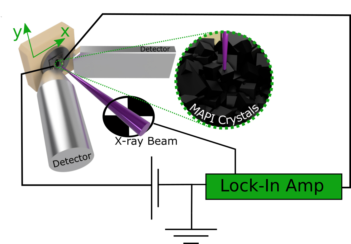
This work investigated the effect of a semiconducting polymer (PCBM) passivating layer on the performance of perovskite X-ray detectors. Perovskite (MAPbI3 – MAPI for short) nanocrystalline films with and without the inclusion of a PCBM layer were studied using X-ray nanoanalysis at beamline ID16B to correlate the elemental distribution, morphology and charge generation and transport at the nanoscale to the device performance on the macroscale. 2D maps of X-ray fluorescence (XRF) and X-ray beam induced current (XBIC) were measured simultaneously. Figure 1 illustrates the experimental setup.
Click image to enlarge
Fig. 1: Diagram showing the experimental setup used at beamline ID16B. The perovskite sample was mounted on an x-y motorised stage. A pink 17.5 keV beam was used, with an X-ray flux of ~8 x 10¹⁰ph/s in a 50 nm spot focused on the sample (smaller than the MAPI nanocrystal size). XRF was measured with two Si-drift detectors and the XBIC signal with a lock-in amplifier and a chopper.
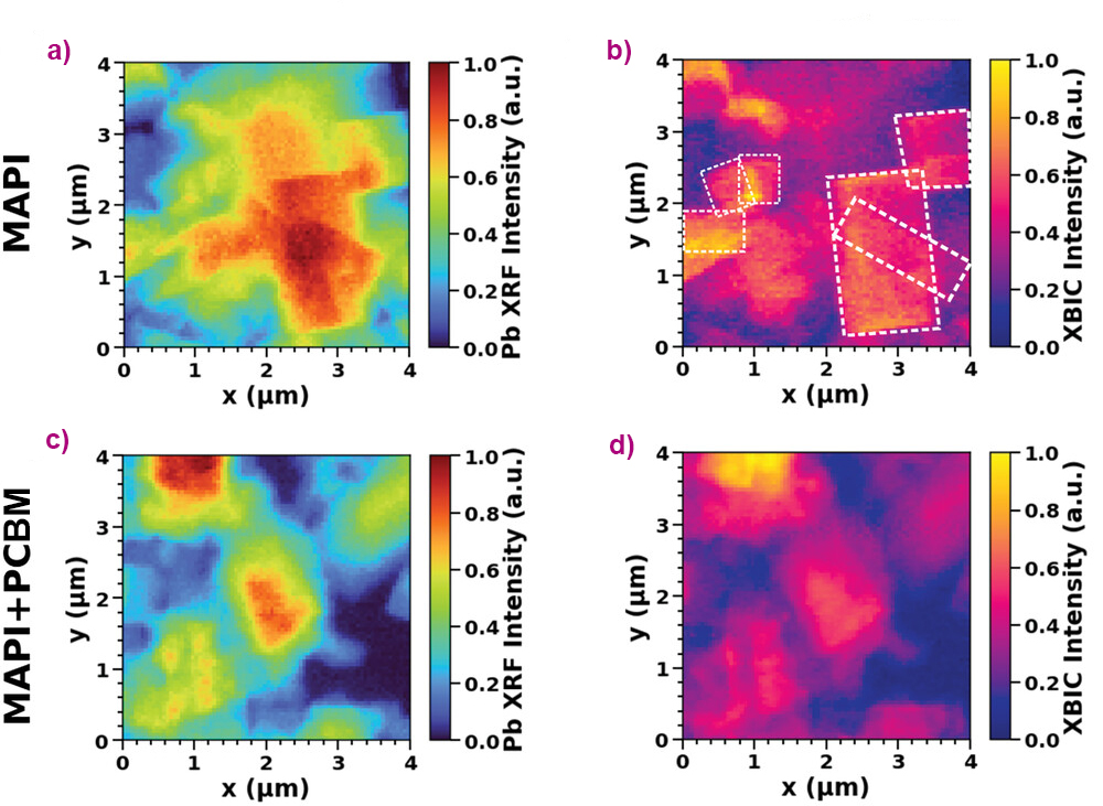
The simultaneous acquisition of XRF and XBIC at the nanoscale made it possible to correlate the elemental distribution and the morphology with the transport and charge collection paths. Figures 2a and b show the representative XRF (Pb distribution) and XBIC data for unmodified MAPI. Variations in the XRF (Pb) signal are due to the non-uniform thickness of the sample, which contained regions with no perovskite grains, regions with single crystalline grains and regions with stacked clustered grains. The XBIC map shows a strong photocurrent signal at the perovskite grain boundaries and a lower signal coming from the bulk region (which instead exhibits higher Pb XRF intensity) of each microcrystal. The missing correlation between the XRF and XBIC maps in unmodified MAPI suggests that photogenerated charge collection is different between the boundaries of the grains and the rest of crystallite volume.
Figures 2c and d show the representative XRF and XBIC data for the MAPI + PCBM samples. While in the unmodified MAPI the XBIC signal is consistently higher at the perovskite grain boundaries than in the middle of the grains, in the MAPI + PCBM sample, the XBIC signal is uniform over the entire active volume. The average output current density was found to be higher for the MAPI + PCBM sample than for unmodified MAPI, confirming that the improved performance with the addition of the organic semiconductor is also valid at the nanoscale. The spatial correlation between XRF and XBIC signals was found to be higher for the MAPI + PCBM sample, with the entire active volume contributing to charge generation and collection uniformly and efficiently.
Click image to enlarge
Fig. 2: a) Pb XRF map in a 4 µm × 4 µm area, normalised to (0,1) for unmodified MAPI sample. b) XBIC map at 1 V for MAPI acquired in the same region as in (a): the boundaries of the perovskite grains are highlighted by dashed white lines. c) XRF and (d) XBIC maps for the MAPI + PCBM sample acquired in the same region.
Based on these results, the following mechanism was proposed: (i) for unmodified MAPI, a higher gain is present at the grain boundaries due to a higher defect concentration; (ii) in MAPI + PCBM, the organic semiconductor passivates the traps at the grain boundaries and acts as a sink for electrons, which are then transported to the electrodes via the PCBM, while the holes are transported via the perovskite layer. Due to the large difference in the electron and hole mobility, a charge unbalance is generated which, in turn, activates a higher gain in the whole active volume of the detector.
These results demonstrate that X-ray nanoanalysis is a powerful tool to investigate perovskite detectors and to build a bridge between processes that take place at the nanoscale and the macroscopic device performance. The understanding of these effects at the nanoscale allows the manufacture of more sensitive and more reliable thin film perovskite X-ray detectors.
Principal publication and authors
X-ray nanoanalysis revealing the role of electronically active passivation layers in perovskite X-ray film detectors, M. Verdi (a), A. Ciavatti (a), J. Segura-Ruiz (b), L. Basiricò (a), R. Sorrentino (c), I. Gonçalves (c,d), A. Petrozza (c), F. Boscherini (a), B. Fraboni (a), Adv. Electron. Mater., 2201346 (2023); https://doi.org/10.1002/aelm.202201346
(a) Department of Physics and Astronomy, University of Bologna, Bologna (Italy)
(b) ESRF
(c) Center for Nano Science and Technology@PoliMi, Istituto Italiano di Tecnologia, Milano (Italy)
(d) Physics Department, Politecnico di Milano, Milano (Italy)
References
[1] A. Ciavatti et al., Adv. Funct. Mater. 31, 2009072 (2021).
| About the beamline: ID16B |
|
ID16B is a hard X-ray nanoprobe dedicated to 2D or 3D analysis of nano-scaled materials combining X-ray fluorescence (XRF), diffraction (XRD), absorption spectroscopy (XAS), excited optical luminescence (XEOL), X-ray beam induced current (XBIC) and phase-contrast imaging. Low temperature, in-situ or operando sample environments can be accommodated. ID16B is dedicated to research areas with high scientific and societal impacts such as nanotechnology, earth and environmental sciences, and bio-medical research. |
partners


European Synchrotron Radiation Facility - 71, avenue des Martyrs, CS 40220, 38043 Grenoble Cedex 9, France.