- Home
- News
- Spotlight on Science
- Sweeping transformation...
Sweeping transformation to metallic phase following laser excitation in titanium pentaoxide
26-02-2021
In the quest to understand and control material transformation with light, scientists have used time-resolved powder X-ray diffraction at beamline ID09 to study the semiconducting-to-metal phase transitions in sub-micron crystals of titanium pentaoxide (Ti3O5) in unprecedented spatial and temporal detail.
Materials with properties that can be transformed by using external control parameters such as temperature, pressure, or light are of great interest for technological applications, for example, optical and heat storage. Light control of material properties, made possible by the development of intense pulsed lasers, promises faster switching and the possibility of exploring non-equilibrium states of matter. One of the main challenges in ultrafast material science is to trigger phase transitions, such as the semiconductor-to-metal transition, with short pulses of light. It is therefore of utmost interest to be able to observe ultrafast structural changes induced by photoexcitation of a material.
Unfortunately, this comes with extreme theoretical and experimental challenges, exemplified by the semiconducting-to-metal phase transitions in sub-micron crystals of titanium pentaoxide (Ti3O5). In this material, the absorption of photons causes the transfer of electrons into empty orbitals well localised in so-called ‘Ti-Ti dimers’. Less than one microsecond later, the sample is found with a good fraction of metallic phase. Previous studies have described strain propagation [1,2,3], but without the complexity of simultaneous phase transition. On the other hand, studies of Ti3O5 have lacked either the time resolution [4] or the structural sensitivity [5] to observe strain wave propagation and its role in the phase transition, so the cascade of events leading to such dramatic changes has thus far eluded understanding.

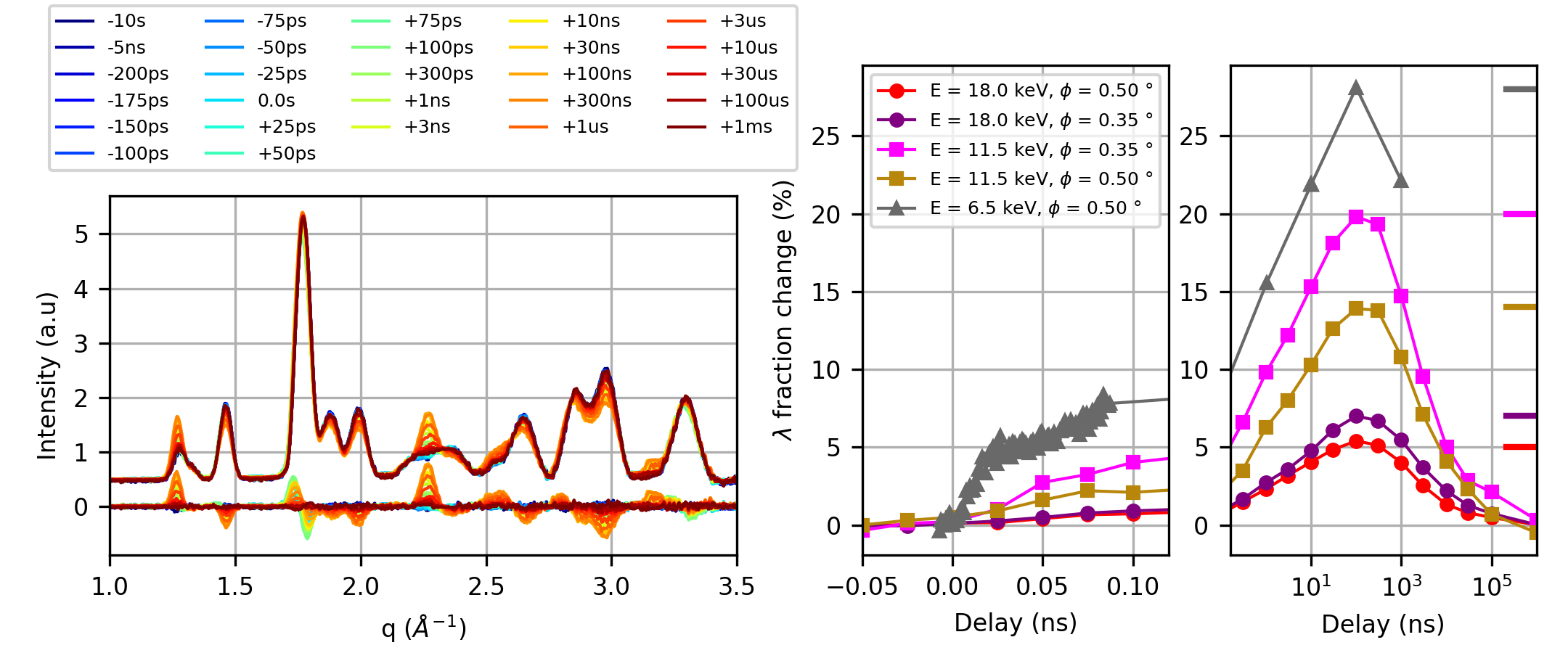
Fig. 1: Time-resolved XRD patterns obtained at beamline ID09. The different photon energy and grazing incidence angles are used to obtain different sensitivity to surface and bulk, resulting in the full characterisation of thermal diffusion in the sub-μm length scale. Much higher quality data are today achievable with EBS.
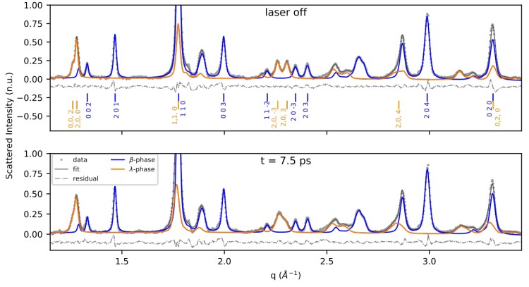
Researchers prepared a pellet of Ti3O5 nanocrystals with an abundance of the semiconducting phase and excited it with a laser while employing time-resolved powder X-ray diffraction (XRD) at beamline ID09 (Figure 1) and the SwissFEL Free Electron Laser (Figure 2) to measure the lattice deformation in the phase transition as a function of time, on time scales of femtoseconds to microseconds. The high-quality powder X-ray diffraction patterns allowed for full Rietveld refinement for both phases, thus providing an extremely detailed picture both structurally and temporally and allowing the researchers to observe a three-step transformation pathway for the semiconducting-to-metal transition.
First, within a few hundreds of femtoseconds, and before the unit cell has had time to move, local structural changes driven by the electronic changes caused by photon absorption are observed. These local structural changes build up local stress that propagates with the speed of sound (strain waves), transforming the uppermost 100 nm of the sample. During the last step, heat diffusion drives transformation of the bulk material (not directly exposed to light). The strain and the phase transition propagate at the same velocity, and clearly precede the thermal diffusion homogenisation, showing that the strain wave determines the pathway of a truly macroscopic semiconductor-to-metal transition in nanomaterials that exhibit a volume change during the phase transition.

Fig. 2: Femtosecond XRD data, obtained at SwissFEL, revealing the build-up of local stress triggered by electronic excitation.
This non-destructive approach opens up fascinating prospects for an advanced degree of strain control through electronic and structural precursors, and offers a new perspective for ultrafast control of materials with evidence of a strain wave pathway for achieving a phase transition in nanocrystallites excited by a light pulse. The higher focusing capabilities and the increased spectral brightness of the Extremely Brilliant Source (EBS) will likely contribute to the wider applicability of such techniques.
Principal publication and authors
Strain Wave Pathway to Semiconductor-to-Metal Transition Revealed by Time-Resolved X-ray Powder Diffraction, C. Mariette (a), M. Lorenc (a), H. Cailleau (a), E. Collet (a), L. Guérin (a), A. Volte (a), E. Trzop (a), R. Bertoni (a), X. Dong (a), B. Lépine (a), O Hernandez (b), E. Janod (c), L. Cario (c), V. Ta Phuoc (d), S. Ohkoshi (e), H. Tokoro (e,f), L. Patthey (g), A. Babic (g), I. Usov (g), D. Ozerov (g), L. Sala (g), S. Ebner (g), P. Böhler (g), A. Keller (g), A. Oggenfuss (g), T. Zmofing (g), S. Redford (g), S. Vetter (g), R. Follath (g), P. Juranic (g), A. Schreiber (g), P. Beaud (g), V. Esposito (g,*) Y. Deng (g), G. Ingold (g), M. Chergui (h), G.F. Mancini (g,h), R. Mankowsky (g), C. Svetina (g), S. Zerdane (g), A. Mozzanica (g), A. Bosak (i), M. Wulff (i), M. Levantino (i), H. Lemke (g), M. Cammarata (a,**), Nat. Commun. (2021); http://doi.org/10.1038/s41467-021-21316-y
(a) Univ. Rennes, CNRS, IPR (Institut de Physique de Rennes) - UMR 6251, Rennes (France)
(b) Univ. Rennes, CNRS, ISCR (Institut des Sciences Chimiques de Rennes) - UMR 6226, Rennes (France)
(c) Institut des Matériaux Jean Rouxel (IMN), Université de Nantes, CNRS, Nantes (France)
(d) GREMAN – UMR 7347 CNRS, Université de Tours, Tours (France)
(e) Department of Chemistry, School of Science, University of Tokyo, Tokyo (Japan)
(f) Department of Materials Science, Faculty of Pure and Applied Sciences, University of Tsukuba,
Ibaraki (Japan)
(g) SwissFEL, Paul Scherrer Institut (PSI), Villigen (Switzerland)
(h) Laboratory of Ultrafast Spectroscopy, Lausanne Center for Ultrafast Science (LACUS), École Polytechnique Fédérale de Lausanne, Lausanne (Switzerland)
(i) ESRF
(*) Current address: Stanford Institute for Materials and Energy Science, Stanford University and SLAC National Accelerator Laboratory, Menlo Park, California (USA)
(**) current address: ESRF
References
[1] C. Thomsen et al., Phys. Rev. B 34, 4129-4138 (1986).
[2] D Schick et al., Struct. Dyn. 1, 064501 (2014).
[3] P. Ruello & V.E. Gusev, Ultrasonics 56, 21-35 (2015).
[4] K.R. Tasca et al., Chem. Phys. Chem. 18, 1385 (2017).
[5] A. Asahara et al., Phys. Rev. B 90, 014303 (2014).


