- Home
- News
- Spotlight on Science
- Understanding hybrid...
Understanding hybrid halide perovskite thin layers to improve solar cell efficiency
22-04-2022
Scientists have carried out X-ray diffraction and microscopy experiments at beamline ID01 to study the microstructure of hybrid halide perovskite solar cells, namely texture and strain. A deeper insight into the microstructure is essential to be able to control it; and could ultimately lead to methods to engineer it in order to improve solar cell performance.
Share
Hybrid halide perovskite (HHP) solar cells are the newest addition to different photovoltaic technologies developed over the past 10 years, with the efficiencies of these devices having increased to reach values close to those of silicon-based solar cells, at around 25.5%.
However, a number of issues need to be addressed in order to increase the performances of these devices. The effect of the presence of strain in the perovskite layer is still under debate, with large inconsistencies in the literature [1], while the orientation of the perovskite lattice, or texture, can also affect its physical and mechanical properties [2].
In this work, scientists carried out X-ray diffraction (XRD) and full-field diffraction X-ray microscopy (FFDXM) experiments at beamline ID01 to study the structure of HHP thin layers at the microscale, in order to understand the mechanisms governing strain and texture with the perspective of finding ways to engineer the material for higher performance.
Using in-situ X-ray diffraction, the researchers monitored the strain experienced by a hybrid halide perovskite (MAPbI3) thin layer deposited on a glass substrate covered by an inorganic oxide as it cooled down to room temperature after crystallisation at 100°C. Figure 1 shows the evolution of the lattice parameters of the MAPbI3 film, compared to parameters obtained with bulk MAPbI3 powder.
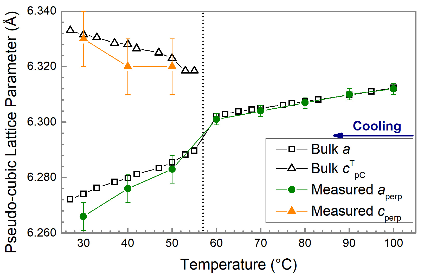
Fig. 1: Evolution of the measured out-of-plane and calculated in-plane lattice parameters of MAPbI3 thin layers during controlled cooling from 100°C to room temperature. The open symbols display the lattice parameters of the unstrained reference sample: MAPbI3 powder and the dotted lines indicate the cubic-tetragonal phase transition temperature in the bulk material (57°C).
The data clearly show that the MAPbI3 layer is mainly relaxed on the substrate, contradicting the commonly accepted hypothesis that strain is present in MAPbI3 layers synthesised above room temperature due to the large mismatch in the thermal expansion coefficients of the perovskite and its substrate. These results demonstrate that there is no direct correlation between this mismatch and the presence of strain in the film.
Grain boundaries might play a key role in the strain relaxation, more particularly combined with the high ion mobility observed in this material, which has been shown to favour the mitigation of lattice defects. However further investigation is required to clearly identify the mechanisms governing the strain behaviour in MAPbI3 layers.
The texture in MAPbI3 layers was then investigated by means of synchrotron full-field diffraction X-ray microscopy (FFDXM) – a powerful technique that enables the direct mapping of crystalline lattices – at beamline ID01, with the aim to understand the nature of a peculiar double lattice orientation that is sometimes observed in MAPbI3(Cl) instead of the more common unique orientation.
MAPbI3 thin layers are generally obtained from a solution of MAI and PbI2 precursors deposited at 100°C. When cooled down to room temperature, they are essentially polycrystalline, with the crystalline direction [00l] lying mainly in the plane of the layer. Some synthesis protocols replace PbI2 by PbCl2, the addition of chlorine being beneficial among other things for the grain size. It also favours a preferential orientation of the crystalline lattice, with a majority texture [hh0] [3]. However, in some cases a double texture [hh0] and [00l] is observed.
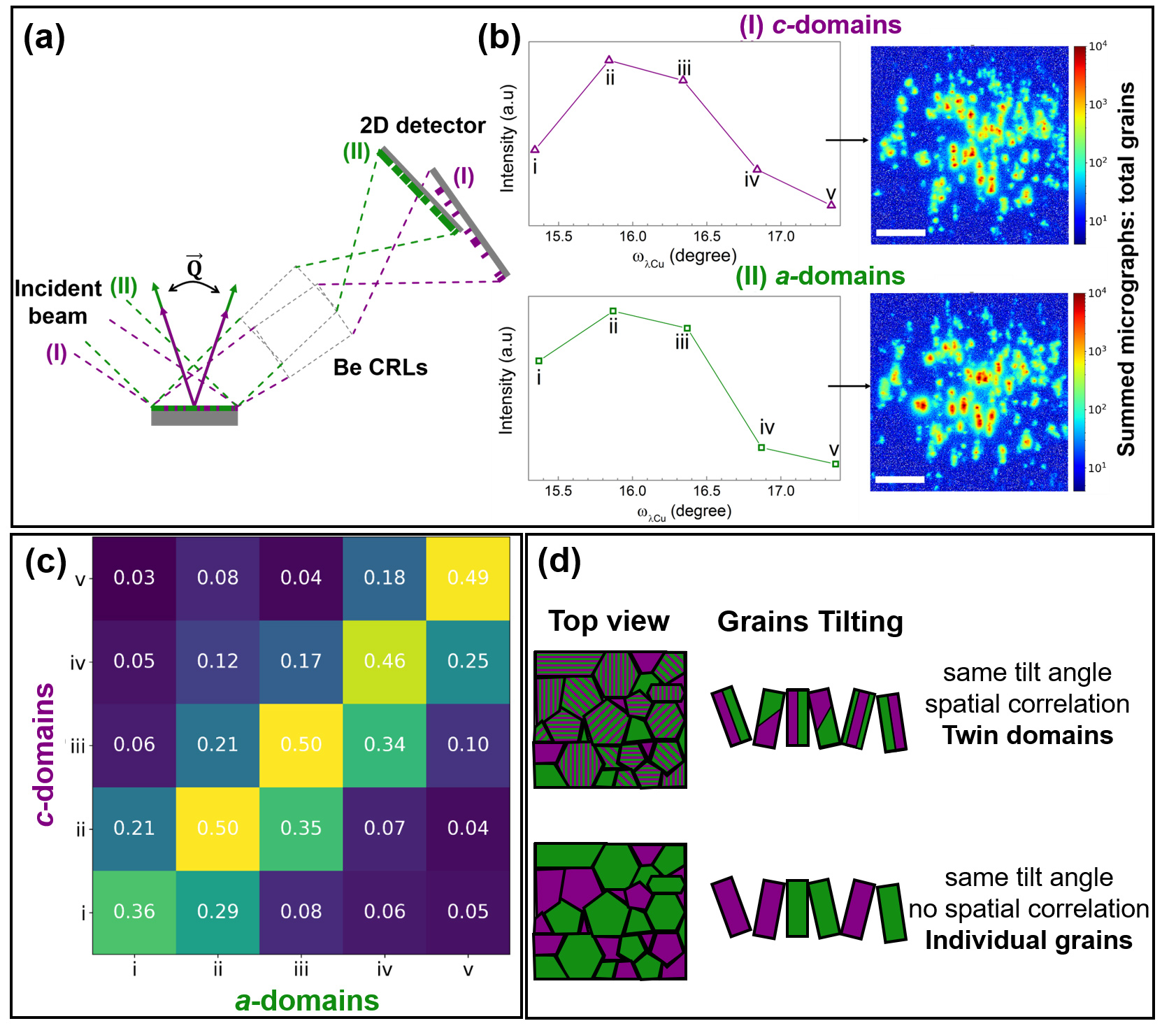
Fig. 2: a) Measurement setup for FFDXM on ID01. b) Obtained rocking curves for both [hh0]-oriented grains (a-domains) and [00l]-oriented grains (c-domains) and resulting summed micrographs. c) Correlation map of a- and c-domains obtained from rocking curve measurements. d) Schematic explaining the conclusion of twin domains. Purple and green colours correspond to c- and a-domains respectively.
The FFDXM results show that these textures are the signature of the presence of ferroelastic twins in the perovskite layer. Indeed, as shown in Figure 2, strong spatial and tilt correlations were evidenced between the distributions of the two [hh0] and [00l] types of grains, demonstrating the presence of twin domains in the grains, which form as the layer experiences a cubic-tetragonal phase transition at around 57°C. Their ferroelastic nature was demonstrated by the observation of the flipping of [00l]-domains into [hh0]-ones under the synchrotron beam, most likely due to the stress induced by the ion migration experienced by the material when exposed to the beam.
The stability of the different domain orientations was then investigated by density functional theory (DFT) calculations. PbI2-terminated surfaces were found to favour the [hh0] orientations while, for MAI-terminated ones, both [hh0] and [00l] domains were equally stabilised. This shows that the chemical nature of the terminations can drive the orientation of the crystallites, illustrating the determining role of the chemical environment at the film-substrate interface.
Taken together, these different results constitute an important advance in understanding the microstructure of hybrid halide perovskite layers, paving the way to methods of engineering them to enhance their optoelectronic properties, device performance and stability.
Principal publication and authors
Microstructure of Methylammonium Lead iodide Perovskite Thin Films: A Comprehensive Study of the Strain and Texture, A.A. Medjahed (a), T. Zhou (b), J.C. Alvarez Quiceno (c,d), P. Dally (e,f), P. Pochet (d), T.U. Schülli (g), D. Djurado (a), P. Reiss (a), S. Pouget (d), Adv. Energy Mater. 2103627 (2022); https://doi.org/10.1002/aenm.202103627
(a) University Grenoble Alpes, CEA, CNRS, IRIG, SyMMES, Grenoble (France)
(b) Center for Nanoscale Materials, Argonne National Laboratory, Lemont, Illinois (USA)
(c) Instituto de Fisica, Universidad de Antioquia UdeA, Medellin (Colombia)
(d) University Grenoble Alpes, CEA, IRIG, MEM, Grenoble (France)
(e) Institut Lavoisier de Versailles (ILV), Univ. Versailles Saint-Quentin-en-Yvelines, Univ. Paris-Saclay, CNRS, Versailles (France)
(f) IPVF, F-91120, Palaiseau (France)
(g) ESRF
References
[1] D. Liu et al., Nat. Mater. 20, 1337-1346 (2021).
[2] P. Zhao et al., Mater. Today Energy 17, 100481 (2020).
[3] M. Bouchard et al., J. Phys. Chem. C 121, 7596-7602 (2017).
partners


European Synchrotron Radiation Facility - 71, avenue des Martyrs, CS 40220, 38043 Grenoble Cedex 9, France.