- Home
- News
- Spotlight on Science
- Fast diffraction...
Fast diffraction imaging for nano- and micro- electronics and functional materials
01-08-2014
An optimised quick mapping technique (K-Map) has been put into service at ID01, the ESRF’s beamline for diffraction imaging, during the current refurbishment of this beamline. This enhancement of the beamline makes it capable of rapidly accessing structural properties such as lattice tilt, strain, composition and thickness fluctuations, without any surface or morphological limitations. The new instrumentation comprises a structural scanning probe microscope and its control system. This fast imaging technique provides exceptional strain sensitivity and resolution and can be applied to any crystalline object, even polycrystalline thin films, which constitute the majority of electronic devices and functional materials.
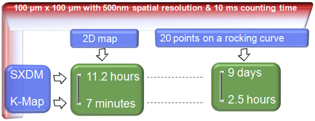
The study of individual nanostructures using a focused X-ray beam poses a number of experimental challenges. The first challenge is the localisation of the structure. For this, scanning X-ray diffraction microscopy (SXDM) offers a real space mapping of the sample that facilitates the localisation of nanostructures. The second challenge is related to the scanning time. Common beamline control programs, such as SPEC [1] at the ESRF, offer a variety of scan modes that are implemented in software such as step-scans, i.e. sequences of distinct motor positioning and photon counting. The weak point of this scanning mode is the dead time required for positioning of hardware and software triggering (data transfer, connection between the control programme, the motors and the detectors). Solving this issue can considerably reduce the measurement time, which allows many more measurements to be made during an experiment. For the K-Map technique, the standard controlling software SPEC of the detector and the piezo stage has been replaced by a hardware control system (MUSST [2]), eliminating the positioning time and reducing the SXDM time considerably (Figure 1).
 |
|
Figure 1. Example showing the gain in time between SXDM and K-Map. |
Two-dimensional quick continuous mapping of a sample at a given reciprocal space position can thus be performed with sub-micrometre resolution. Real space maps are produced by continuously moving the sample while recording scattering images with a fast 2D detector for every point along a rocking curve. Five dimensional data sets are then produced containing millions of detector images (current data flow of 10 TB/day). The images are processed by a user friendly X-ray strain and orientation calculation software (XSOCS) [3], developed at ID01, for automatic analysis. XSOCS separates tilt from strain and generates 2D maps of these parameters. It can be used to extract preliminary results during an experiment, which gives the user the opportunity to adjust the strategy for the experiment. In addition, the application of such fast scanning methods offers the possibility of performing operando studies at high temperatures or in gas or liquid environments.
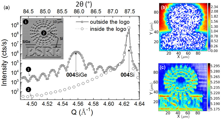
As a test sample, an ESRF logo was printed on a 40 nm Si0.8Ge0.2 layer grown on a Si (001) substrate (see inset Figure 2a) using a focused ion beam (FIB) at IHP.
 |
|
Figure 2. (a) θ-2θ scans around the 004 Si and Si0.8Ge0.2 Bragg reflections outside and inside the structured ESRF logo. Inset: SEM image of the sample. (b) Integrated intensity at the 004 Si0.8Ge0.2 Bragg position. (c) 2D plot of the integrated intensity in the vicinity of the 004 Si Bragg peak (diffuse scattering). |
Using XSOCS to plot the intensity distribution in real space for selected regions in reciprocal space renders a first qualitative analysis which can be achieved quickly because it is efficient in terms of computer processing. This supplies multiple structure-sensitive contrast channels going far beyond traditional imaging by scanning electron microscopy. Figure 2b shows the 004 diffracted intensity from the Si0.8Ge0.2 decreasing significantly in the area inside the logo. This is a direct measure of the damage done to the crystal structure (rendered amorphous) during the FIB process. Although the structured sample surface is still clearly visible on the SEM image (inset Figure 2a), K-Mapping proves here to be highly sensitive to the sample crystallinity and allowed the detection of the structure quality (such as epitaxial quality and degree of poly-crystallinity) inside the nanometric volumes defined by the beam.
The 2D map of the integrated intensity in the vicinity of the 004 Si Bragg reflections clearly resolves the ESRF logo (Figure 2c). The non-homogeneous distribution indicates the presence of structural inhomogeneities, e.g. crystalline mosaicity or strain distribution. The calculation and the decoupling of strain and lattice tilt, for each position (x, y) on the sample is also carried out by the XSOCS software and yields additional information.
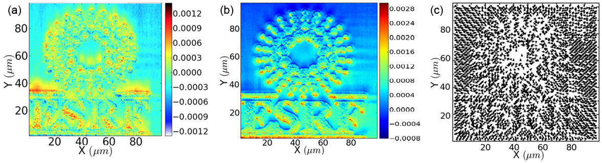
The 2D plot of the strain distribution (Figure 3a) shows that the Si layer underneath the Si0.8Ge0.2 structured logo remains slightly strained (<0.0015%) after the FIB process. Nevertheless, strain is not the only structural FIB-induced effect. The Si {001} planes show slight tilts, up to 0.0024°, under the structured Si0.8Ge0.2 area (Figure 3b). Figure 3c shows that under the structured Si0.8Ge0.2, the FIB process does not induce any preferential orientation.
 |
|
Figure 3. 2D maps of (a) the out-of-plane strain component and (b) the tilt magnitude (°), as a function of the beam position on the sample. (c) Directional representation (arrows), of tilted {001} atomic planes with respect to the sample surface normal. |
The 2D plots created by the K-Map technique are proof that lattice variations and tilts of the order of Δa/a < 10-5 and 10-3°, respectively, still produce significant contrast. Heterogeneous materials, including most microelectronic devices, present weak structural variations that affect their performances. Accessing these weak but significant variations is therefore of great importance.
Principal publication and authors
Imaging of strain and lattice orientation by quick scanning X-ray microscopy combined with three-dimensional reciprocal space mapping, G.A. Chahine (a) M.-I. Richard (b,a), R.A. Homs-Regojo (a), T.N. Tran-Caliste (a), D. Carbone (a) V.L.R. Jacques (a), R. Grifone (a) P. Boesecke (a), J. Katzer (c), I. Costina (c) H. Djazouli (a), T. Schroeder (c) and T.U. Schülli (a), Journal of Applied Crystallography 47, 762 (2014).
(a) ESRF
(b) Aix-Marseille Université, CNRS, IM2NP UMR 7334, Marseille (France)
(c) Innovations for High Performance Microelectronics, Frankfurt (Germany)
References
[1] Certified Scientific Software, PO Box 390640, Cambridge, MA 02139, USA.
[2] http://www.esrf.eu/Instrumentation/DetectorsAndElectronics/musst
[3] https://sourceforge.net/projects/xsocs/files/
Top image: 2D map of the tilt magnitude (up to 0.0024°) of the Si {001} atomic planes with respect to the surface for a FIB etched image on a 40 nm Si0.8Ge0.2 layer grown on Si.
partners


European Synchrotron Radiation Facility - 71, avenue des Martyrs, CS 40220, 38043 Grenoble Cedex 9, France.