- Home
- News
- Spotlight on Science
- Ferroelectric domain...
Ferroelectric domain supercrystals
09-03-2021
Ferroelectric materials exhibit complex domain structures that can be controlled by tailoring their electrical or mechanical boundary conditions. In artificially layered superlattices composed of ultrathin metallic and ferroelectric layers, the three-dimensional ordering of ferroelectric domains leads to a domain ‘supercrystal’.
Share
Over the last two decades, ferroelectric domains and domain walls have proven to be a fascinating playground for exploring novel ways of creating functional materials and devices [1]. Individual domain walls, where the local symmetry is different from the bulk, can host properties that are radically different from those of the host material. For example, ferroelectric domain walls can be orders of magnitude more conducting than the domains they separate, offering the prospect of transient or reconfigurable electronics where individual conducting elements are created and destroyed at will by the application of an electric field. Another route to novel functionalities is to exploit the collective dynamics of domain walls in dense domain structures. Domain walls in heterostructures of ultrathin ferroelectrics exhibit highly inhomogeneous patterns of rotating dipoles that are not possible in bulk materials. The dynamics of these domain walls can lead to extremely large permittivities and even to so-called negative capacitance behaviour [2].
Much of the research on such domain patterns has focused on superlattices consisting of alternating ultrathin ferroelectric and dielectric layers, where the dielectric layers introduce a discontinuity in the ferroelectric polarisation and induce the formation of domains that minimise the electrostatic energy of the system. The resulting dense, periodic nanodomain patterns and their response to external stimuli are especially well-suited for characterisation using diffraction techniques [3,4]. However, the response of such domain patterns to the presence of free carriers has been much less well explored.
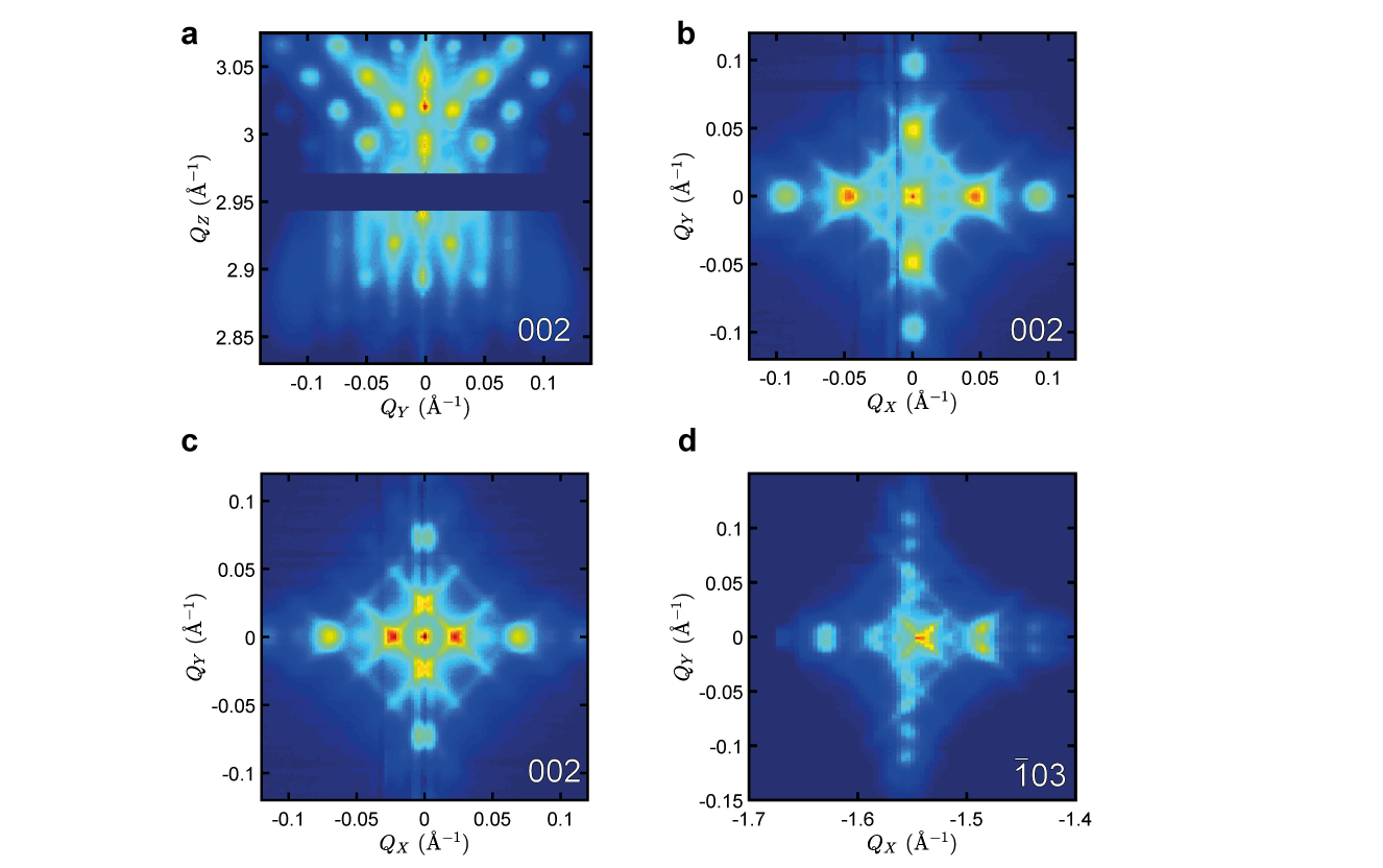
In this work, domain formation in superlattices consisting of ferroelectric PbTiO3 and metallic SrRuO3 layers deposited on DyScO3 substrates was investigated using a combination of synchrotron X-ray diffraction experiments at beamlines ID01 and BM02, combined with piezoresponse force microscopy, transmission electron microscopy and phase-field modelling. Despite the presence of metallic screening, the ferroelectric layers in all superlattices were found to form domains with no net out-of-plane polarisation, due to the imperfect screening of the polarisation at the metal-ferroelectric interfaces [5]. However, while superlattices with thinner ferroelectric layers exhibited signatures of regular vortex-like domain structures confined to individual ferroelectric layers, in samples with thicker layers, a very different domain structure appears, doubling the superlattice periodicity along the out-of-plane direction (Figure 1). The very sharp peaks of this periodic structure indicate that this new phase is highly ordered in all three directions and is coherent across the entire thickness of the superlattice.

Fig. 1: X-ray diffraction signatures of the supercrystal phase. Reciprocal space maps in the (a) QY-QZ and (b,c) QX-QY planes around the 002pc Bragg peak of a PbTiO3/SrRuO3 superlattice, with sharp satellite peaks due to the highly ordered three-dimensional domain structure. d) Reciprocal space map in the QX-QY plane around the 1 ̅03pc Bragg peak showing satellites that arise due to a complex tilt pattern.
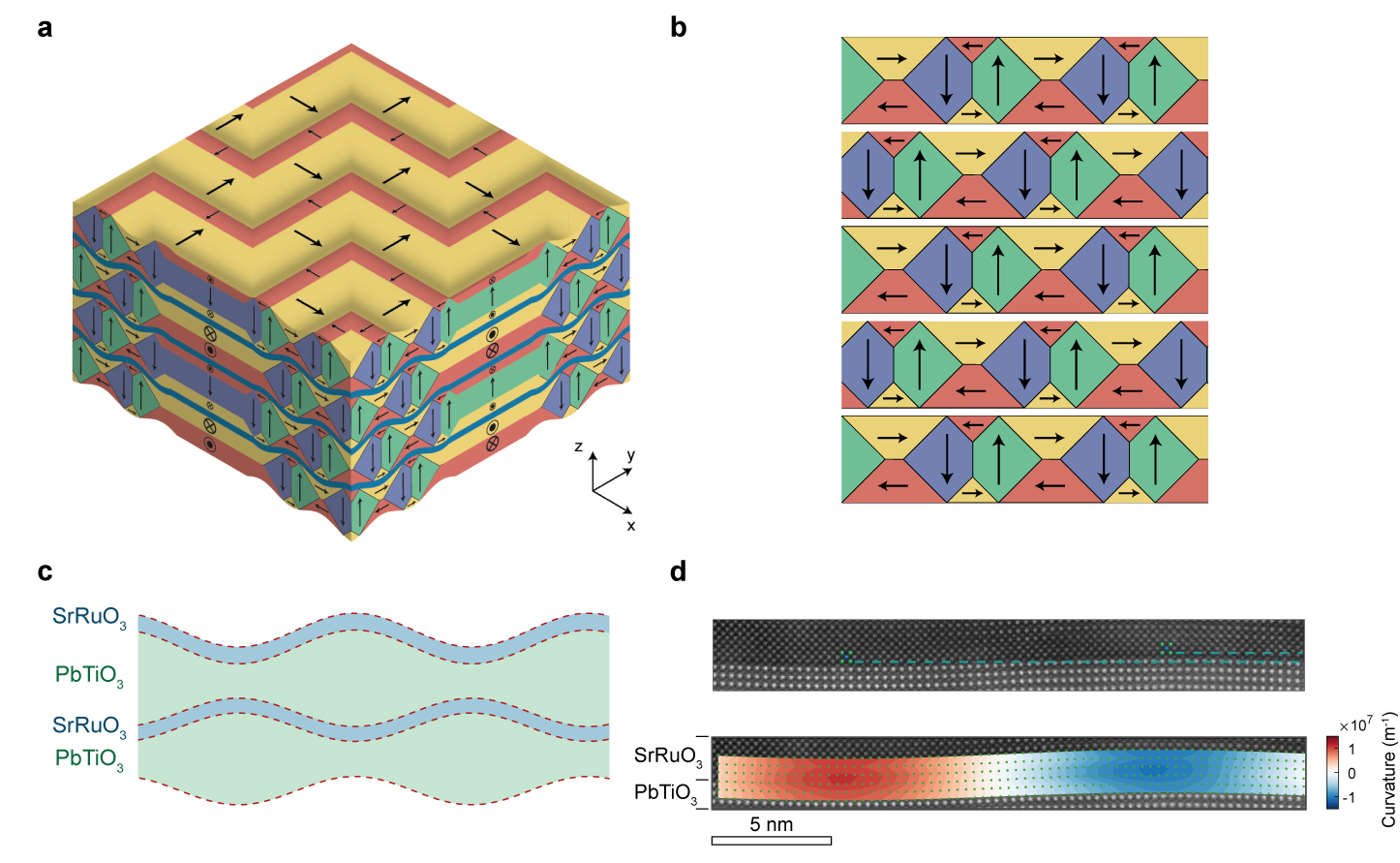
To understand the 3D polarisation arrangement giving rise to this complex reciprocal space structure, the superlattices were further investigated using piezoresponse force microscopy and scanning transmission electron microscopy. Combining the information from these three different techniques reveals a highly ordered domain ‘supercrystal’ structure, shown in Figures 2a and 2b. This polarisation pattern is in excellent agreement with phase field simulations, which further reveal that in an applied field, domain-wall displacements in the supercrystal give rise to an enhancement of the dielectric constant in the ferroelectric layers along all three spatial directions. Furthermore, the supercrystal structure was found to appear independently of the type of spacer layer, and has been observed in superlattices where the metallic SrRuO3 is replaced with insulating SrTiO3, or fine-period PbTiO3/SrTiO3 spacers.
The supercrystal structure appears in order to minimise both the electrostatic and the elastic energy. The tensile misfit strain imposed by the substrate favours a structure with alternating in-plane and out-of-plane polarisations separated by {110} domain walls. However, a non-zero out-of-plane component of the polarisation cannot be maintained within individual layers due to the poor screening at the ferroelectric-metal (or ferroelectric-dielectric) interfaces. The ferroelectric layers thus split into in-plane and out-of-plane flux-closure domains, as shown in Figure 2b. This domain structure is characterised by periodic deformations, with alternating expansion and contraction of the lattice, to minimise the misfit strain imposed by the substrate as well as the electrostatic energy cost associated with a single out-of-plane polarisation. These expansions and contractions couple through the whole superlattice and create a three-dimensional domain structure.

Fig. 2: a) Sketch of the three-dimensional domain structure, with arrows indicating the directions of the spontaneous polarisation within each domain. b) Two-dimensional sketch showing the alternating in-plane and out-of-plane flux-closure domains that lead to the distortions summarised in (c). d) Top: High-resolution scanning transmission electron microscopy image of the interfaces between PbTiO3 and SrRuO3 showing the bending of the lattice. Bottom: Local curvature in each atomic plane.
Importantly, the coupling between the different ferroelectric layers results in periodic bending of the SrRuO3 spacer layers in order to match the deformation of the PbTiO3 layers. This imposes very large curvatures of the order of 107 m-1 that lead to large strain gradients in the metallic layers (Figures 2c and 2d). Strain gradients naturally break inversion symmetry in any material and can lead to a range of novel properties, including large flexoelectric response in semiconductors, bulk photovoltaic effect in non-ferroelectric materials and interesting transport properties in metallic systems. Because the curvature of spacer layers is induced by the ferroelectric domain structure, it can be modified using electric fields. Therefore such supercrystals, combining ferroelectric materials with different spacer materials, provide a new way to manipulate the electronic structure of a large range of oxides and to explore a variety of strain gradient-induced phenomena.
Principal publication and authors
Metal-ferroelectric supercrystals with periodically curved metallic layers, M. Hadjimichael (a,b), Y. Li (a), E. Zatterin (a,c), G.A. Chahine (c,d), M. Conroy (e), K. Moore (e), E.N. O’Connell (e), P. Ondrejkovic (f), P. Marton (f), J. Hlinka (f), U. Bangert (e), S. Leake (c), P. Zubko (a), Nat. Mater. (2021); https://doi.org/10.1038/s41563-020-00864-6.
(a) London Centre for Nanotechnology and Department of Physics and Astronomy, University College London (UK)
(b) Department of Quantum Matter Physics, University of Geneva (Switzerland)
(c) ESRF
(d) Université Grenoble Alpes, CNRS, Grenoble (France)
(e) Department of Physics, Bernal Institute, University of Limerick (Ireland)
(f) Institute of Physics of the Czech Academy of Sciences, Prague (Czech Republic)
References
[1] G. Catalan et al., Rev. Mod. Phys. 84, 119-156 (2012).
[2] J. Íñiguez et al., Nat. Rev. Mater. 4, 243-256 (2019).
[3] M. Hadjimichael et al., Phys. Rev. Lett. 120, 037602 (2018).
[4] P. Zubko et al., Phys. Rev. Lett. 104, 187601 (2010).
[5] M. Hadjimichael et al., Phys. Rev. Mater. 4, 094415 (2020).


