- Home
- Counting dislocations in micro-crystals using coherent X-ray microdiffraction
Counting dislocations in micro-crystals using coherent X-ray microdiffraction
For semiconductor device miniaturisation to reach the nanoscale, one of the most important challenges is to obtain perfectly crystalline micro- or nano-crystals. Any deviation from the perfect atomic arrangement constitutes a ‘defect’ that can dramatically reduce the performance of a device. This is especially true for the so-called ‘phase’ defects such as dislocations that induce a shift of one part of the crystal with respect to another. A technique that can directly evaluate the number of defects in a device is thus highly desirable. But estimating the amount of defects in a non-destructive way is challenging, especially in the case of low defect density. In this work, we show that coherent X-ray diffraction can provide an answer to this important material science problem thanks to its high sensitivity to “phase” defects in crystals.
 |
|
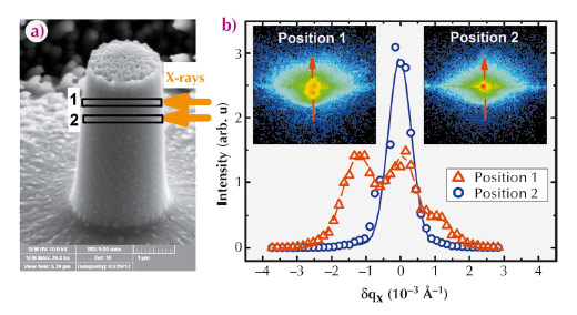
Fig. 113: a) Scanning electron microscopy image of the pillar studied here. The volumes probed at positions 1 and 2 are indicated. b) Insets: Coherent diffraction patterns on the 202 Bragg reflection recorded at positions 1 and 2. Graph: Projection of the patterns along vertical direction of the detector. |
We have studied an InSb micropillar (Figure 113a) in which lattice defects were induced in a controlled way via mechanical deformation up to the early plastic regime using a nano-indenter [1]. Only a few (partial) dislocations are expected to appear from this deformation, leaving stacking faults that induce a phase shift of adjacent parts of the crystals of 4π/3 in the direction [101]. We used a focused coherent beam at beamline ID01, using slits to select the coherent part of the beam and Fresnel Zone Plates to obtain a 200 (v) x 500 (h) nm2 beamsize. Diffraction images on the 202 Bragg reflection were measured with a Maxipix 2D pixel detector at different positions of the pillar. A sharp Bragg reflection was found at most positions (e.g. position 2 in Figure 113b), but several maxima were found at a specific position of the pillar (position 1, Figure 113b). The sharp peak measured at position 2 accounts for a perfect crystalline arrangement in the sample, while several peaks recorded at position 1 are interferences due to the defects induced in the pillar, namely the phase shifted regions separated by stacking faults [2].
 |
|
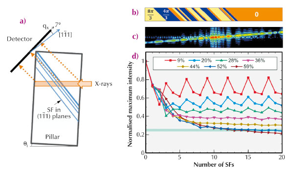
Fig. 114: a) Geometry of pillar, stacking faults (SF), and scattering. b) Simulation of the phase of the illuminated sample volume with 20 defects (SFs), located in a volumic fraction V = 50%. c) Calculated coherent diffraction pattern corresponding to the volume displayed in a). d) Maximum intensity of the diffraction patterns calculated with increasing number of defects in different fractions of illuminated volume. The blue straight line represents the maximum intensity recorded during the experiment in the defected part relatively to the one measured in the perfect regions. |
Simulations were performed to estimate the number of stacking faults contained in the volume probed at position 1. They take into account the geometry of the experiment (Figure 114a). Figure 114b displays a computed real space phase configuration in which N=20 defects have been randomly inserted in a fraction V = 50% of the total illuminated volume. Adjacent volumes separated by a defect are phase-shifted by 4π/3. The corresponding calculated diffraction pattern is displayed in Figure 114c. Several peaks due to complex interferences are visible on this pattern, as measured in the experiment. However, varying the number of defects and the size of the defected volume can lead to qualitatively similar diffraction patterns, which makes it impossible to retrieve the exact real space configuration of the stacking faults in the illuminated volume. This problem is well know for the imaging of crystals by phase retrieval algorithms. Interestingly, we found that the maximum intensity on the diffraction pattern is extremely sensitive to the number of defects and to the defected volume size, especially for small numbers of defects, as shown in Figure 114d. This behaviour allowed us to evaluate the number of dislocations and the size of the defected volume at position 2 of the investigated sample (N~15 defects in V~50%).
Coherent X-rays can thus be exploited not only to reveal the presence of crystal defects but to quantify them, i.e. estimate their number and the size of the defected volume. This approach can be used to relate the devices performance with the presence and extent of defects in a crystalline micro-structure.
Principal publication and authors
V.L.R. Jacques (a), D. Carbone (a), R. Ghisleni (b) and L. Thilly (c), Physical Review Letters 111, 065503 (2013).
(a) ESRF
(b) Laboratory for Mechanics of Materials and Nanostructures, EMPA, Swiss Federal Laboratories for Materials Testing and Research, Thun (Switzerland)
(c) Institut PPrime, CNRS-University of Poitiers-ENSMA, SP2MI, Futuroscope (France)
References
[1] L. Thilly, R. Ghisleni, C. Swistak and J. Michler, Philosophical Magazine 92, 3315 (2012).
[2] V.L.R. Jacques, S. Ravy, D. Le Bolloc’h, E. Pinsolle, M. Sauvage-Simkin and F. Livet, Physical Review Letters 106, 065502 (2011).
partners


European Synchrotron Radiation Facility - 71, avenue des Martyrs, CS 40220, 38043 Grenoble Cedex 9, France.