- Home
- News
- Spotlight on Science
- Synchrotron-radiation...
Synchrotron-radiation Computed Laminography
10-08-2006
Synchrotron-radiation computed laminography is a new technique for the non-destructive 3D imaging of flat laterally-extended objects with spatial resolution reaching the micrometre scale.
Share
Current development in computed tomography (CT) with synchrotron radiation (SR) aims to increase the spatial resolution. One constraint, however, is the field of view of the detector, which is limited by the finite number of detector pixels. This limits the spatial dimensions of the object to be imaged and a sample has to be cut from the region of interest of a larger object. In other words, high resolution CT permits non-destructive quality inspection only for devices smaller than the detector's field of view. Restricting the size of the sample to the micrometre range poses major problems for certain types of materials both in sample preparation and for structural stability during the tomographic scan. Furthermore, the imaging of laterally-extended objects suffers from a large variation of the beam transmission while rotating the object in a CT experiment leading to imaging artefacts. To overcome these limitations, synchrotron-radiation computed laminography (SRCL) was developed [1]. SRCL allows high-resolution non-destructive 3D imaging of regions of interests in flat but laterally-extended objects and devices which may include sensors, flip-chip devices and other microsystems.
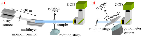
Feasibility experiments at the ESRF beamlines ID19 and ID15 were carried out in a collaboration between ANKA/ISS (Forschungszentrum Karlsruhe, Germany), University of Karlsruhe, the German Fraunhofer Association and the ESRF Imaging Group. The SRCL method consists of the acquisition of projection data sets similar to standard CT, but with a rotation axis that is inclined at an angle  < 90° instead of being perpendicular to the incoming beam like standard CT (see Figure 1). When the device normal is aligned approximately parallel to the inclined rotation axis, the integral X-ray transmission onto the 2D detector does not change considerably during sample rotation. In particular this avoids projections with missing information where the integral transmission would tend to zero due to a long beam path within the sample.
The technological potential of SRCL for high-resolution non-destructive applications has already been demonstrated [2]. In particular, electronic devices were investigated with monochromatic as well as with white synchrotron radiation, providing detailed information about their interconnection technology. In comparison to laboratory methods, SRCL benefits additionally from the specific qualities of synchrotron radiation such as high photon flux, low angular divergence and high partial coherence in combination with high flux.
 |
|
Fig. 1: Comparison between the experimental setups for (a) computed tomography, and (b) computed laminography, at ESRF beamline ID19. |
The example selected in Figure 2 illustrates the capabilities for 3D imaging of flip-chip bonded devices. After bump bonding, the flip-chip solder joints are no longer accessible for visual inspection. Image (a) shows a 3D rendition of bump bonds, cut open in a plane parallel to the substrate. Voids are clearly visible in the interior of the bump bonds. Such voids affect the long-term reliability of the device when it is exposed to heating/cooling cycles, e.g. due to device operation. Images (b) and (c) are reconstructed cross-sectional slices showing a number of large and small voids, the latter predominantly at the interface to the integrated circuit's metallisation layers (top part in b). The Pb-rich phase of the solder is also clearly visible in slice (c), and so are solder splashes near the bump bonds (small satellite spots). Slice (d) highlights a detail of the metallisation and conduction lines on the integrated circuit's surface towards the bonding/substrate side.
 |
|
Fig. 2: SRCL inspection of a flip-chip bonded device (experiment performed on ID15A). (a) 3D rendition of some bump bonds at a device corner; two mutually perpendicular slices, (b) perpendicular and (c) parallel to the device surface. Internal voids affecting the reliability of the device are clearly discernible. The coloured image (d) features a detail of metallisation layers and conduction lines (see arrows) on the hidden surface of the IC. Voxel size is 1.6 µm, X-ray energy range is approx. 30 to 50 keV (white beam). |
In summary, SRCL provides a unique tool for non-destructive imaging of flat, laterally-extended objects with spatial resolution reaching the µm scale. With the current tendencies towards nanoscale imaging and the associated decrease in the field of view (of 100 µm or less) on the sample, SRCL is expected to alleviate non-destructive sample preparation since deposition of thin layers on planar substrates could be less demanding for sample stability than the extraction of thin rods with similar diameters.
A dedicated laminography setup is scheduled to be installed at ID19 in August 2006. It has been designed to be compatible with ID15 so that highly-absorbing objects can be efficiently scanned using high X-ray energies. One of the target application fields is research and development in microsystem technology (MST) encompassing the design, processing, production and application of technical systems, which, by miniaturisation of their components, contain structures of sizes down to the (sub-)µm scale integrated in devices of macroscopic dimensions.
References
[1] L. Helfen, T. Baumbach, P. Mikulík, D. Kiel, P. Pernot, P. Cloetens and J. Baruchel, Appl. Phys. Lett. 86, 071915 (2005).
[2] L. Helfen, A. Myagotin, P. Pernot, M. DiMichiel, P. Mikulík, A. Berthold, T. Baumbach, Nucl. Instr. Meth. A, 563, 163-166 (2006).
Authors
L. Helfen (a,b), T. Baumbach (a), A. Myagotin (a), P. Mikulík (c), D. Kiel (a), P. Pernot (a,b), M. DiMichiel (b), P. Cloetens (b) and J. Baruchel (b).
(a) ISS/ANKA, Forschungszentrum Karlsruhe (Germany)
(b) ESRF
(c) Institute of Condensed Matter Physics, Masaryk University, Brno (Czech Republic)
partners


European Synchrotron Radiation Facility - 71, avenue des Martyrs, CS 40220, 38043 Grenoble Cedex 9, France.