New XBIC setup at BM05 allows coupled characterisation of semiconductor crystals
A new X-ray beam-induced current (XBIC) technique implemented at beamline BM05 allows the evaluation of the local detection efficiency of crystals used as detectors. Coupled with diffraction topography measurements, these quantitative imaging tools can help industrial teams to optimise their semiconductor crystal growth and processes.
Share
The development of semiconductor-based detectors requires new tools to better characterise the electronic properties of semiconductor samples. The X-ray beam-induced current (XBIC) technique, which had already been used successfully at beamline ID21 to study diamond crystals for medical application detectors [1], as well as at ID16B for solar cells [2], has been implemented as an industrial tool at beamline BM05, as part of the IRT NanoElec project.
With the technique, a bias voltage is applied between the two electrodes and the XBIC is read out thanks to pico-ammeters. A 10-keV, 15-µm-diameter X-ray beam is used, focused by beryllium lenses, which displays a photon flux 80 times higher than the direct beam. Scanned samples are translated along the vertical and horizontal directions, and 2D maps can be obtained of the XBIC current for different crystal type and thicknesses (down to 50 µm).
Click to enlarge
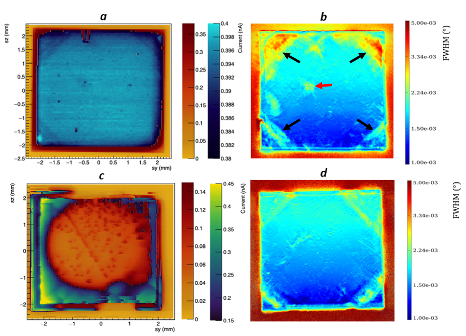
Fig. 1: a) XBIC map for a 500-µm thick diamond. b) FWHM X-ray RCI map of the same sample as in (a). The red arrow shows a bunch of dislocations and the black arrows show growth sector boundaries. c) XBIC map for a 150-µm diamond from the same batch but irradiated with 68 MeV protons. d) FWHM X-ray RCI map of the same sample as in (c).
The setup was commissioned by characterising a series of diamond crystals, which were metallised on both sides at the Institut Néel. Figure 1 shows the XBIC and the transmission Rocking Curve Imaging (RCI) [3] maps at 20 keV for two single-crystal CVD diamonds from the same batch; the first was unprocessed and the second was irradiated with a total fluence of 6.3x10¹⁴ 68-MeV-protons.cm-2 at ARRONAX facility.
The first sample (Figure 1a) shows a rather uniform XBIC response. The corresponding RCI full-width half maximum (FWHM) map (Figure 1b) shows growth sectors and dislocations (indicated by arrows), and allows these features to be correlated to a percent level XBIC signal variation. The second sample shows an efficiency of charge collection four times lower in the irradiated area (3-mm diameter) than in the rest of the crystal (Figure 1c). However, the RCI map (Figure 1d) indicates that the FWHM in this area is not higher than the one measured on the non-irradiated sample. This shows that the XBIC and the RCI techniques provide complementary information, and suggests a low-damage irradiation of the crystal itself and an origin of the irradiation-related XBIC signal degradation that is not associated to crystalline defects.
Click to enlarge
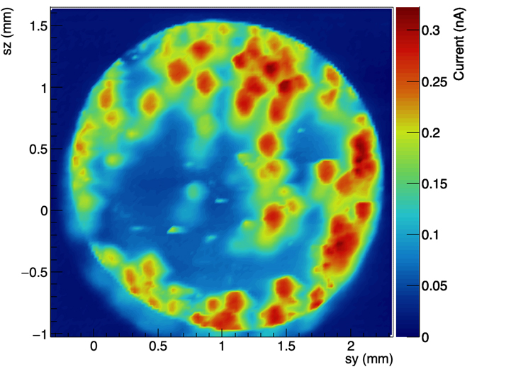
Fig. 2: XBIC map of a diamond grown on iridium.
Figure 2 shows the XBIC map for a more unconventional diamond crystal grown on an iridium substrate. Some parts of the crystal show high charge collection efficiency, while it is very low on the rest of the sample: this could result from an inhomogeneous growth of the diamond crystal. Similar observations are obtained for polycrystalline samples where the heterogeneity is even larger.
The XBIC setup is a very valuable tool for the characterisation of the electronic properties of semiconductor samples. Its location at beamline BM05 offers the possibility to couple the XBIC maps to diffraction topography measurements. These quantitative imaging tools can help industrial teams to optimise their semiconductor crystal growth and processes. The XBIC setup will be available to our industrial partners at the beginning of 2023.
Authors
F. Lafont, T. N. Tran Caliste, J. Baruchel, E. Capria. ESRF.
References
[1] M-L Gallin Martel et al., (2017); https://hal.archives-ouvertes.fr/PRIMES/hal-01436786v1
[2] C. Ossig et al., (2019); https://dx.doi.org/10.3791/60001
[3] T-N Tran Thi et al., J. Appl. Cryst. 50, 261-569 (2017).
partners


European Synchrotron Radiation Facility - 71, avenue des Martyrs, CS 40220, 38043 Grenoble Cedex 9, France.