- Home
- News
- Spotlight on Science
- Polarity domains...
Polarity domains in GaN wires mapped at the nanoscale
06-04-2017
GaN nanowires have potential to improve the performance of light emitting diodes. The optical properties of a device based on nanowires are highly dependent on the growth conditions of the nanowires. X-ray excited optical luminescence microscopy has been used to map single GaN wires and reveal the influence of silane injection during growth on the material quality.
Share
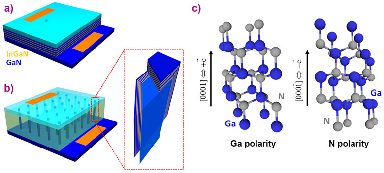
GaN is the main semiconductor used for the fabrication of visible light LEDs. The traditional LED structure is composed of a 2D stack of alternating GaN and InGaN layers a few nanometres thick (Figure 1a). Electrons and holes injected into such a structure recombine radiatively in the InGaN layers with the emission of light at a wavelength determined by the indium content and layer thickness. Such a structure, however, suffers from a high number of defects due to the lattice mismatch and from a strong internal electric field along the c growth axis that reduces the LED efficiency. Nanowires are an alternative to the traditional layered structure that could solve such issues. They can be grown on highly mismatched substrates, and their side facets can be used to deposit core/shell InGaN/GaN heterostructures, increasing the total emitting surface substantially with a drastic reduction of the impact of the internal electric field (Figure 1b). Although nanowires are being used as the basis for LED devices, the characterisation of their structural, electrical and optical properties is still a challenge at the nanoscale. Here, we studied GaN wires grown by metal organic vapour phase epitaxy (MOVPE) using two nanoimaging tools available at beamline ID16B: X-ray fluorescence (XRF) and XEOL [1].
 |
|
Figure 1. a,b) Schematics of 2D and wire based LED structures; c) Wurtzite GaN structure with Ga and N polarity. |
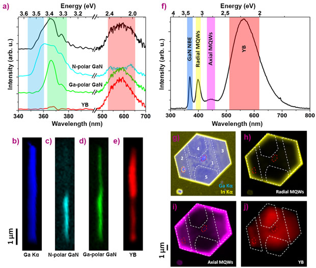
In standard growth conditions GaN crystallises in the wurtzite structure which is not centro-symetric: the growths along the +c (Ga-polarity) and –c (N-polarity) axis are not equivalent (Figure 1c). As a result, the dopant incorporation and chemical reactivity are different for these two polarities. Here, we used the fact that Ga- and N-polar GaN incorporates Si differently to map the presence of these two domains in single wires. The growth of these GaN wires by MOVPE requires the injection of silane, resulting in a high Si dopant concentration (> 1019 cm-3) [2]. Depending on electron carriers provided by Si, the GaN near band edge (NBE) light emission is therefore shifted compared to undoped GaN due to band filling effect (Burstein-Moss effect) [3]. The analysis of the XEOL spectra obtained from single dispersed GaN wires shows the presence of three contributions: two GaN NBE emission peaks around 370 nm attributed to the different Si content in Ga- and N-polar GaN, and the defect associated yellow band (YB) centred around 550 nm (Figure 2a). Figure 2c-e displays their spatial variations within a single wire. The N-polar GaN emission is mainly present in the bottom part of the wire grown under high silane flow. The upper part of the wire, on the other hand, grown without silane injection shows an increase of the defect band intensity and a decrease of the other contributions, suggesting a reduction of the material quality. The evolution of these two polarity domains can be followed along the wires with nanoscale resolution. Our findings reveal the coexistence of both Ga- and N- polar domains in these samples that could be controlled by specific surface preparation. The fabrication of such predetermined polarity domains in tunable shapes could lead to even more applications and functionalities.
We also studied core/shell InGaN/GaN wires from the top facets by XRF and XEOL to gain information about the influence of polarity on the indium distribution and on the emission of InGaN/GaN multi quantum wells (MQWs). From a large defective wire (Figure 2g), we can clearly observe the core/shell structure with a very intense indium fluorescence signal surrounding the hexagonal wire. The XRF map has been divided into five regions with different indium depositions. Figure 2f shows the complete XEOL spectrum with four main contributions attributed to GaN NBE, radial MQWs, axial MQWs and yellow band. A close inspection of the axial MQWs shows that their intensities are maximum in regions 2 and 3, as well as in region 1 at a lower level. No light attributed to MQWs originates from regions 4 and 5, but the defect related emission becomes stronger there. This suggests significant variations in the top facet MQWs possibly related to material quality and facets orientation.
The simultaneous measurement of XRF and XEOL provided an insight into the influence of growth conditions on GaN polarity of individual wires and on the InGaN and MQWs through indium deposition quality. The combination of these two techniques at the nanoscale presents many advantages to be further used in the study of even more complex semiconductor nanostructures with chemical and optical selectivity.
Principal publication and authors
Silane-induced N-polarity in wires probed by a synchrotron nanobeam, D. Salomon (a), A. Messanvi (b,c), J. Eymery (b,d), G. Martinez-Criado (e), Nanoletters 17, 946-952 (2017); doi: 10.1021/acs.nanolett.6b04291.
(a) ESRF
b) Equipe mixte CEA-CNRS-UJF Nanophysique et semiconducteur, Grenoble (France)
c) Institut d’electronique fondamentale, Paris (France)
d) CEA, INAC-MEM, Nanostructures and synchrotron radiation laboratory, Grenoble (France)
e) Instituto de cienca de materiales de Madrid, Madrid (Spain)
References
[1] G. Martinez-Criado et al., J. Synchrotron Radiat. 23, 344-352 (2016).
[2] D. Salomon et al., Nanosccale Res. Lett. 8, 61 (2013).
[3] P. Prystawko et al., Phys. Status Solidi B 210, 437 (1998).


