- Home
- Modelling of the MTF performance of high spatial resolution X-ray detectors
Modelling of the MTF performance of high spatial resolution X-ray detectors
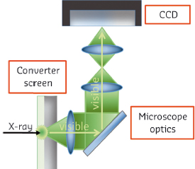
X-ray detectors for high spatial resolution imaging are mainly based on indirect detection. The detector consists of a converter screen made of a scintillating material, light microscopy optics and an imaging sensor (CCD or CMOS). The scintillating screen converts part of the absorbed X-rays into a visible light image, which is projected onto the CCD by means of the optics (Figure 153). The performance of the detector is strongly influenced by the properties of the converter screen, which include X-ray absorption, spread of energy deposition, scintillation yield and emission wavelength.
 |
|
Fig. 153: Schematic of a detector for high spatial resolution based on indirect detection. |
To obtain detectors with micrometre and sub-micrometre spatial resolution, thin (1-50 µm) single crystal film (SCF) scintillators are required.
At the ESRF, X-ray imaging applications regularly make use of energies up to 120 keV. At relatively high energies, the efficiency of the detector is reduced dramatically because of the weak absorption of the converter screen. For example, at 20 keV a 5 µm thick scintillator of gadolinium gallium garnet (GGG) absorbs only 10% of the incident photons. Furthermore, the low stopping power degrades the spatial resolution because of the energy deposition spread in the converter screen.
At the ESRF, GGG and LSO (lutetium orthosilicate) scintillators are produced by liquid phase epitaxy (LPE). Additionally, the development of new scintillating materials is currently being investigated: the goal is to improve the contradictory compromise between absorption and spatial resolution, thereby increasing the detection efficiency while keeping a good image contrast even at high energy. The development of a new kind of scintillating screen by LPE is time consuming and expensive. Therefore, we developed a “simulation tool” able to predict the optimal combination of scintillating screen (in terms of thickness, composition and substrate) and visible light optics for different energy ranges. The aim of these simulations is to guide the choice of the materials that will be developed by LPE.
We combined a Monte Carlo approach using Geant4 Monte Carlo toolkit [1] for the energy deposition leading to light emission with analytical calculations for the optical collection. The energy spread in the converter screen is described by Monte Carlo simulations in which a monochromatic X-ray pencil beam hits the scintillator, generating secondary X-rays and electrons. To quantify the spatial resolution, we estimated from the spatial distribution of the deposited energy the linear spread function (LSF). We also calculated the modulation transfer function (MTF) corresponding to the LSF in the frequency domain: this function gives the contrast as function of the spatial frequency.
However the intrinsic MTF of the converter screen does not describe the ultimate resolution of the detector completely: the visible light still needs to be projected on a CCD by means of microscope optics. The optics magnify the image, reducing the real pixel size of the CCD, with the consequence that it can degrade the resolution because of the combination between the depth of field of the optics and the thickness of the scintillator. This means that part of the visible image produced in the screen will be projected on the image sensor as a defocused image, creating a blur in the final image. To include this effect, we applied analytical equations describing the optics to the MTF of the converter screen obtained by Monte Carlo simulations [2].
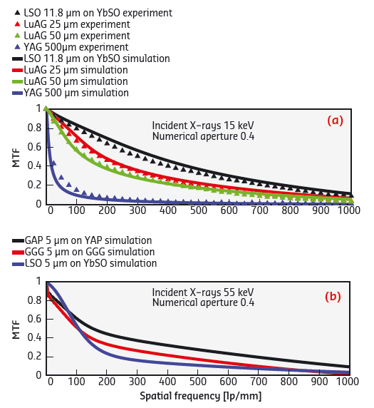
We validated our model experimentally at beamline BM05, using the slanted edge method [3] to investigate the spatial resolution of the detector in a variety of configurations. In Figure 154a we show the excellent agreement between experimental MTF and the simulated MTF obtained at 15 keV. The microscope optic has a numerical aperture of 0.4 and it was combined with various scintillators: LSO grown by LPE on YbSO substrate (ytterbium orthosilicate), yttrium and lutetium aluminium garnet (LuAG and YAG) bulk single crystals grown by the Czochralski technique. The thickness of the scintillators ranges from 11.8 µm to 500 µm. In Figure 154b, the same model is used to simulate the MTF at 55 keV: gadolinium aluminum perovskite (GAP), a candidate material for the development by LPE, is compared to LSO and GGG, both currently used at ESRF. Simulations show that GAP could improve the spatial resolution compared to the available screens in the energy range higher than the gadolinium k-edge.
 |
|
Fig. 154: Contrast as a function of the spatial frequency (MTF): a) X-rays 15 keV, experimental data and simulations; b) X-rays 55 keV, simulations for different materials. |
A model for indirect detection has been developed and validated with experimental data. The agreement with experiment is very good and we are confident that our model can be used for optimisation of detectors, helping to estimate the spatial resolution for different configurations of the detector for various experimental conditions. Additionally, it gives important information about the improvements that could be obtained regarding resolution and efficiency using a new scintillator or a new detector configuration as well as the crucial role of the substrate when the ultimate resolution is desired.
Authors
F. Riva (a,b), P.A. Douissard (a), T. Martin (a) and C. Dujardin (b).
(a) ESRF
(b) ILM, Université Lyon 1-CNRS (France)
References
[1] S. Agostinelli et al., Nuclear Instruments and Methods A 506, 250-303 (2003).
[2] H.H. Hopkins, Proc. R. Soc. Lond. A 231, 91-103 (1955).
[3] Slanted Edge MTF: http://rsb.info.nih.gov/ij/plugins/se-mtf/index.html
partners


European Synchrotron Radiation Facility - 71, avenue des Martyrs, CS 40220, 38043 Grenoble Cedex 9, France.