- Home
- Users & Science
- Scientific Documentation
- ESRF Highlights
- ESRF Highlights 2012
- Dynamics and extreme conditions
- Disentangling bulk and surface electron screening behaviour in (Ga,Mn)As
Disentangling bulk and surface electron screening behaviour in (Ga,Mn)As
The worldwide effort to understand the mechanisms at the origin of ferromagnetic order in diluted magnetic semiconductors (DMS) has resulted in a wealth of new concepts in spintronics. In the case of (Ga,Mn)As, fundamental questions persist regarding the spatial homogeneity of the coupling between Mn ions and the influence of surface and interface effects on the bulk electronic properties [1,2]. Recent advances in research on diluted magnetic semiconductors have demonstrated that the properties of the first few atomic layers play a fundamental role for future spintronics applications, hence, the understanding and control of the carrier density in (GaMn)As may have great technological significance. While many experimental and theoretical efforts have focused on reaching a reliable control and description of surface and interface effects of DMS, a basic understanding of the differences between surface and bulk electronic properties is still lacking.
Within an international collaboration, we performed high-resolution hard X-ray photoemission spectroscopy (HAXPES) at SPring-8 beamline BL15XU and at ESRF beamline ID16 on well-characterised (Ga,Mn)As films. Thanks to the unusually high bulk sensitivity achieved by HAXPES (probing depth > 100 Å), the presence of a distinct electronic screening channel in the bulk, hitherto undetected in surface sensitive analysis, has been revealed, thus demonstrating that the electronic structure of the bulk and the surface of (Ga,Mn)As is profoundly different. Comparison with model calculations identifies the character of the Mn 3d electronic states and clarifies the role of hybridisation in mediating the ferromagnetic coupling.
 |
|
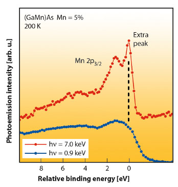
Fig. 39: Mn 2p3/2 photoemission spectra from a (Ga,Mn)As film (5% Mn, Tc = 60 K), after HCl chemical etching, measured using soft and hard X-ray energies. Spectra have been aligned to the same relative binding energy scale without background subtraction. |
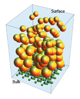
Figure 39 compares soft X-ray (surface sensitive) and HAXPES (bulk sensitive) Mn 2p spectra of (GaMn)As. The surface sensitive spectrum agrees well with previous Mn 2p PES reports [3]. In contrast, the Mn 2p HAXPES spectrum reveals an additional sharp feature at the onset of the main 2p3/2 peak which is completely absent in the surface-sensitive one. Similar low binding energy peaks have recently been reported in HAXPES from 3d-based transition metal oxides, and are generally associated with a metallic-like, i.e. delocalised, character [4]. Using model calculations we were able to ascribe these changes to the electron screening process, which highlights the importance of the d-electron hybridisation. Figure 40 explains the difference in the screening ability of the electrons: each Mn atom carries a cloud of partially localised d electrons. A difference in the spatial extension of the electronic cloud, which is indicated by a change in the radius of the sphere, corresponds to a different hybridisation. Near the surface the d electrons are more localised (smaller radius) than in the bulk (larger radius), corresponding to a different screening ability, a fundamental parameter to set ferromagnetism in the system.
 |
|
Fig. 40: The (GaMn)As electronic structure. Randomly-substituted Mn atoms on the Ga sites are shown at the bottom of the figure. The electronic clouds of partially localised Mn d electrons are approximated by spheres, with a radius proportional to the screening length. Near the surface (top) the d electrons are more localised (smaller radius) than in the bulk (bottom, larger radius). |
Our results not only confirm the remarkable change of the screening properties in diluted systems when going from the surface to the volume, but also confirm that adequate knowledge of the electronic structure of the surface/interface in comparison to the bulk one is essential for any real applications.
Principal publication and authors
J. Fujii (a), M. Sperl (b), S. Ueda (c), K. Kobayashi (c), Y. Yamashita (c), M. Kobata (c), P. Torelli (a) F. Borgatti (d), M. Utz (b), C.S. Fadley (e,f), A.X. Gray (e,f), G. Monaco (g), C.H. Back (b), G. van der Laan (h) and G. Panaccione (a), Phys. Rev. Lett. 107, 187203 (2011).
(a) CNR-IOM, TASC Laboratory, Trieste (Italy)
(b) Inst. Experimentelle Physik, Univ. Regensburg (Germany)
(c) NIMS beamline Station at SPring-8, NIMS, Sayo, Hyogo (Japan)
(d) CNR-ISMN, Bologna (Italy)
(e) Dep. of Physics, University of California, Davis (USA)
(f) Material Sciences Division, LBNL, Berkeley, California (USA)
(g) ESRF (h) Diamond Light Source, Chilton, Oxfordshire (UK)
References
[1] T. Dietl, Nature Mater. 9, 965 (2010).
[2] I. Zutic, J. Fabian and S. Das Sarma, Rev. Mod. Phys. 76, 323 (2004).
[3] J. Okabayashi et al., Phys. Rev. B 58, R4211 (1998).
[4] G. Panaccione et al., Phys. Rev. Lett. 97, 116401 (2006).
partners


European Synchrotron Radiation Facility - 71, avenue des Martyrs, CS 40220, 38043 Grenoble Cedex 9, France.