Figure 101
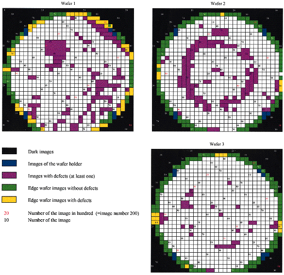
Fig. 101: Typical mappings of the 300 mm Si wafers showing the different distributions of defects.
partners
European Synchrotron Radiation Facility - 71, avenue des Martyrs, CS 40220, 38043 Grenoble Cedex 9, France.
Fig. 101: Typical mappings of the 300 mm Si wafers showing the different distributions of defects.


European Synchrotron Radiation Facility - 71, avenue des Martyrs, CS 40220, 38043 Grenoble Cedex 9, France.