- Home
- Users & Science
- Scientific Documentation
- ESRF Highlights
- ESRF Highlights 2010
- Soft condensed matter
- Biomimetic ultrahydrophobic surfaces for X-ray diffraction studies on biological solution droplets
Biomimetic ultrahydrophobic surfaces for X-ray diffraction studies on biological solution droplets
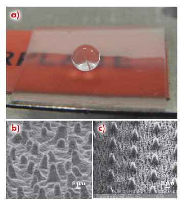
The discovery of super-hydrophobic properties in plant leaves (Lotus effect) [1] has resulted in an intense effort for developing techniques that allow the generation of super-hydrophobic features. Applications of ultra-hydrophobic surfaces (UHS) range from self-cleaning, anti-fouling and anti-wetting textiles, flow-enhancement in microfluidic devices, and recently, even to the biomedical field [2]. Two smart and efficient micro-fabrication techniques have been developed within a collaboration project between the ESRF and two Italian nanofabrication facilities (BIONEM and IIT) to obtain ultrahydrophobic surfaces from commercial flat PMMA sheets with a high X-ray transmission (Figure 64a). The developed surfaces have been fabricated through either a two-step process comprising an optical lithography phase and a plasma etching phase or a single reactive ion etch attack. The similarity between these artificial surfaces and those existing in nature is striking (Figure 64 b,c). With such processing it is possible to make a ready-to-use device in just 12 minutes. Furthermore, the plasma etch technique makes it possible to process several surfaces at the same time.
 |
|
Fig. 64: a) PMMA ultra-hydrophobic surface; b) Features of a Nelumbo Nucifera lotus leaf; c) PMMA micro-structured surface. |
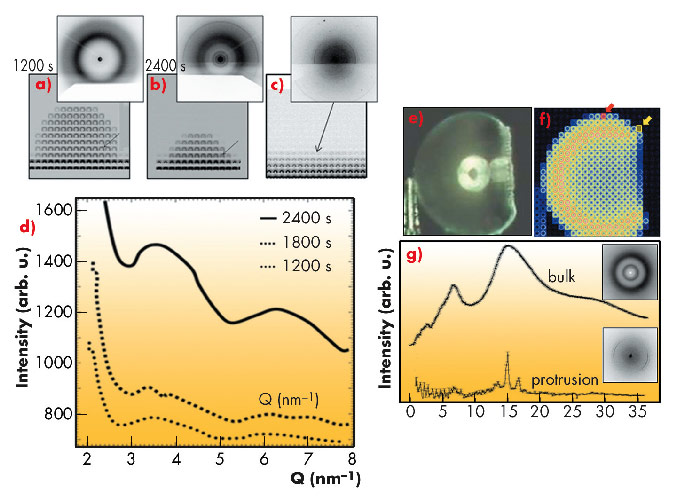
There is currently significant interest in the study of self-assembly processes with the aim of creating novel templates for biofilm deposition, microassay chip manufacturing and other next-generation materials. Materials are usually deposited on surfaces through the drying of solution droplets but microscopic details on deposition processes are often lacking. We have now been able to show that the evaporation of lysozyme (and other biological molecules such as cytochrome C or synthesised peptides [3,4]) solution droplets on ultrahydrophobic PMMA surfaces results in the formation of easily detachable hollow residuals. This is due to the low interaction between the ultrahydrophobic substrate and the aqueous droplets. The process of evaporation of droplets of about 4 µl has been studied in situ by X-ray small- and wide-angle scattering techniques using a beam of about 1 µm (Figure 65 a-d). The SAXS patterns observed at different stages of the evaporation process agree well with simulated lysozyme solution scattering patterns, which is remarkable given the ultra-small volumes probed in a single exposure of < 0.8 pL. An analysis of the diffraction patterns of the solid residuals suggests that the bulk of these hollow residuals is composed of a mixture of about 1/3 < 20 nm nanocrystalline domains and 2/3 short-range order material (Figure 65 e-g). The particle size at the attachment points is about 5 times larger, which is probably due to a shearing process during evaporation.
 |
|
Fig. 65: a-c) Composite raster SAXS/WAXS images of drying lysozyme droplet; d) Azimuthally averaged pattern at selected times after the onset of the drying process; e) Optical image of solidified lysozyme solution droplet residual; f) composite image from 2D raster-scan; g) Upper curve: diffraction pattern from bulk of sphere (red rectangle/arrow in part (f)) and azimuthally averaged pattern. Lower curve: diffraction pattern from protrusion of sphere (yellow rectangle/ arrow in part (f)) and azimuthally averaged pattern. |
The current experiments are a first step towards the integration of an electrode platform to move droplets by means of electrical fields. Indeed such ultrahydrophobic PMMA surfaces represent a potential near contact-free sample support for the study of homogeneous nucleation, chemical reactions and phase transformations in aqueous inorganic and organic solution droplets in combination with SAXS & WAXS µbeam techniques.
Principal publication and authors
A. Accardo (a,b,c), F. Gentile (c,a), F. Mecarini (c,a), F. De Angelis (c,a), M. Burghammer (b), E. Di Fabrizio (c,a) and C. Riekel (b), Langmuir, 26, 15057–15064 (2010).
(a) Center of Bio-Nanotechnology and Engineering for Medicine, University Magna Græcia, Catanzaro (Italy)
(b) ESRF
(c) Italian Institute of Technology, Genova (Italy)
References
[1] C. Neinhuis and W. Barthlott, Ann. Bot. 79, 667–677 (1997).
[2] F. Gentile, G. Das, M.L. Coluccio, F. Mecarini, A. Accardo, L. Tirinato, R. Tallerico, G. Cojoc, C. Liberale, F. De Angelis and E. Di Fabrizio, Microelec. Eng. 87, 798-801 (2010).
[3] A. Accardo, F. Gentile, F. Mecarini, F. De Angelis, M. Burghammer, E. Di Fabrizio, C. Riekel, Microelec. Eng., DOI:10.1016/j.mee.2010.12.044 (2011).
[4] C.A.E. Hauser, R. Deng, A. Mishra, Y. Loo, U. Khoe, F. Zhuang, D.W. Cheong, A. Accardo, M.B. Sullivan, C. Riekel, J.Y. Ying, U.A. Hauser, PNAS, DOI:10.1073/pnas.1014796108 (2011).
partners


European Synchrotron Radiation Facility - 71, avenue des Martyrs, CS 40220, 38043 Grenoble Cedex 9, France.