- Home
- Step-by-step capping of GaN/AlN quantum dots, studied by grazing-incidence anomalous diffraction
Step-by-step capping of GaN/AlN quantum dots, studied by grazing-incidence anomalous diffraction
We report on the investigation of strain and composition of GaN nanostructures (dots) grown on an AlN(0001) epilayer as a function of the thickness of the AlN capping layer, with which the GaN dots were covered after growth. The capping strongly modifies the strain state in the quantum dots (QDs) and therefore plays a decisive role in the modification of the optical properties. Strain is closely related to the composition, shape and aspect ratio of the nanostructures, and on the mutual stress which nanostructures, substrate and the matrix exert on each other.
A model-independent approach can be used to recover the strain and composition by exploiting the chemical sensitivity of resonant elastic X-ray scattering. Two complementary methods, based on resonant X-ray scattering are now available. Multiwavelength anomalous diffraction (MAD) allows an extraction of the scattering amplitude of the resonant atoms (chemical mapping in the reciprocal space) and the diffraction anomalous fine structure (DAFS) spectroscopy that allows a determination of the local environment of atoms located in an iso-strain volume selected by diffraction.
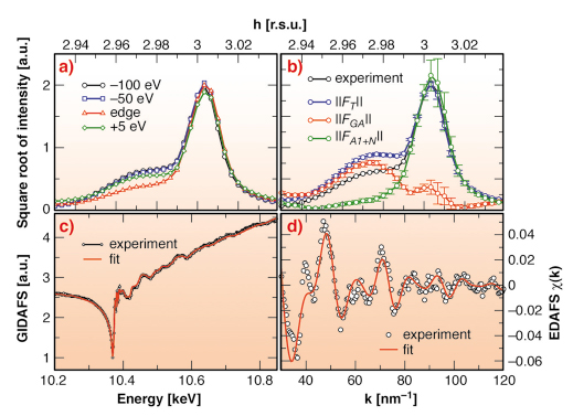
GaN QDs were grown on thin films of AlN on sapphire and on SiC substrates, according to a modified Stranski-Krastanov growth mode. The thickness of the subsequently grown AlN capping layer was in the range of 0-20 monolayers. The average height (diameter) of the free standing nanostructures were found to be 3nm (15 nm) for QDs on AlN/sapphire and 4 nm (30 nm) for QDs on AlN/SiC, respectively. Grazing-incidence MAD (GIMAD) and Grazing-incidence DAFS (GIDAFS) were performed at the Ga K-edge at beamline BM02. Enhanced sensitivity to out-of-plane strain was gained with the sample surface perpendicular to the X-ray beam polarisation vector. We recovered the GaN QDs in-plane strain as a function of AlN cap thickness, by applying the GIMAD method. For this purpose, we measured a set of h-scans (radial scan), close to the in-plane (30-30) Bragg reflection of the AlN substrate with grazing incidence and exit, at 12 different energies. This enabled us to extract the Ga atoms partial structure factor (FGa, Figure 84b) and to determine the average in-plane strain and size of the GaN nanostructures. Out-of-plane strain and the QDs composition were obtained by recording the Extended DAFS oscillations, above the Ga K-edge at the maximum of FGa, in order to probe the QDs core (Figures 84 c,d). The EDAFS oscillations analysis was performed with the IFEFFIT code by fixing the QDs in-plane unit cell parameter (a) to the values found by GIMAD, letting the c parameter vary according to the hexagonal symmetry. For all samples, the Al content was not significant.
 |
|
Fig. 84: Data corresponding to the 10 monolayers AlN coverage. a) experimental intensities measured below (-100 and -50 eV), at the edge, and above (+ 5eV) the Ga K-edge; b) experimental intensities measured at 10.317 keV (50 eV below the Ga K-edge), FGa and FAl+N; c) GIDAFS spectra measured at the maximum of FGa (h = 2.973) together with the best fit obtained with experimental anomalous scattering factors f'Ga and f"Ga of Ga in a GaN thin film. d) experimental EDAFS compared with the best fit. |
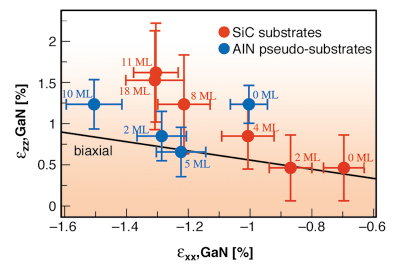
Figure 85 shows the in-plane strain (![]() xx) versus the out-of-plane strain (
xx) versus the out-of-plane strain (![]() zz) for the QD for two kinds of substrates and as a function of the capping layer thickness. The differences between the two series of samples demonstrate the influence of the QDs aspect ratio and the densities of threading edge and misfit dislocations at the AlN/GaN interface on the strain relief mechanism. Finally, the Al fraction as a function of the capping layer thickness, which was obtained by analysing the GIDAFS lineshape (Figure 84c), indicates a wetting of the QDs, followed by a noticeable change in the capping process that corresponds to the filling of the lateral space in between the dots.
zz) for the QD for two kinds of substrates and as a function of the capping layer thickness. The differences between the two series of samples demonstrate the influence of the QDs aspect ratio and the densities of threading edge and misfit dislocations at the AlN/GaN interface on the strain relief mechanism. Finally, the Al fraction as a function of the capping layer thickness, which was obtained by analysing the GIDAFS lineshape (Figure 84c), indicates a wetting of the QDs, followed by a noticeable change in the capping process that corresponds to the filling of the lateral space in between the dots.
 |
|
Fig. 85: GaN QDs strain |
By combining MAD and DAFS, we have systematically determined the in- and out-of-plane strains, as well as the atomic intermixing in the GaN/AlN(0001) nanostructures, as a function of the AlN cap thickness, with a sensitivity to the AlN coverage as small as 2 ML.
Principal Publication and Authors
J. Coraux (a,b), M.G. Proietti (c), V. Favre-Nicolin (a,b), B. Daudin (a), H. Renevier (a,b,*), Phys. Rev. B 73, 205343 (2006); Appl. Phys. Lett. 88, 153215 (2006).
(a) Commissariat à l’Energie Atomique, Département de Recherche Fondamentale sur la Matière Condensée, SP2M, Grenoble (France)
(b) Université Joseph Fourier, Grenoble (France)
(c) Departamento de Fisica de la Materia Condensada, Instituto de Ciencia de Materiales de Aragon, CSIC-Universidad de Zaragoza (Spain)
* Present address : Ecole Nationale Supérieure de Physique de Grenoble, INP Grenoble, MINATEC (France).
partners


European Synchrotron Radiation Facility - 71, avenue des Martyrs, CS 40220, 38043 Grenoble Cedex 9, France.