- Home
- Users & Science
- Scientific Documentation
- ESRF Highlights
- ESRF Highlights 2002
- Surface and Interface Science
- GID Study of Germanium Quantum Dots: Small in Size and High in Density
GID Study of Germanium Quantum Dots: Small in Size and High in Density
During the last 10 years, semiconductor nanostructures have been investigated extensively in order to study the effect of quantum confinement on the physical properties of semiconducting materials. Group IV (i.e. Si and Ge), nanostructures embedded in a dielectric layer can emit light and store carriers suggesting future applications in optoelectronic and non-volatile memory devices.
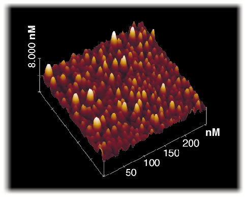
A major difficulty in the fabrication is that nanometric dimensions and high density of dots have to be achieved in order to make the devices operate at room temperature. Recently germanium dots have been grown by Molecular Beam Epitaxy (MBE) on a silicon (001) surface covered by a thin (1.2 nm-thick) silicon oxide and/or silicon nitride layer. Growth has been performed on an MBE machine installed on BM32, the CRG IF beamline. The experimental procedure, which induces the growth of high-density (1011/cm2) and nanometric-size germanium dots on silicon oxide and silicon nitride has been described previously [1,2]. Despite the presence of a thin dielectric layer, germanium dots grown by MBE exhibit an epitaxial relationship with the underlying silicon substrate. In order to optimise the growth procedure a systematic characterisation of the density and shape of dots has been performed by Atomic Force Microscopy (AFM) observations in the Surface Science Laboratory of ESRF (see Figure 34).
 |
|
Fig. 34: Image in tapping mode of germanium dots grown on a silicon (001) surface covered by a thin silicon nitride layer. |
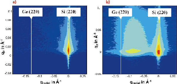
Grazing-incidence X-ray diffraction (GID) experiments have been performed on the ID1 beamline in order to investigate the structural properties of germanium dots, such as size, strain and the orientation relationship to the Si (001) substrate [3].
Several samples have been investigated, consisting of germanium dots with a coverage of 2.2 and 6.6 monolayers, grown through a very thin Si3N4 layer. After annealing at ~710°C, GID measurements were performed at the (220) surface reflection to determine the strain and shape distribution inside the dots.
The radial scans from the (220) germanium to the (220) silicon Bragg peak for the two samples are shown in Figure 35. For small dots (a few nm, resulting from 2.2 ML of Ge) only a small asymmetry can be detected close to the silicon Bragg peak (Figure 35a) indicating a high degree of pseudomorphic strain inside the dots. Larger dots (~12 nm, resulting from 6.6ML of Ge) exhibit a distribution of in-plane lattice parameter induced by an elastic strain relaxation and/or silicon interdiffusion into the Ge dots (Figure 35b).
 |
|
Fig. 35: qradial/qz reciprocal space maps close to the Si (220) surface reflection: (a) sample with 2.2 ML of Ge. (b) sample with 6.6 ML of Ge grown on a silicon (001) surface covered by a thin silicon nitride layer. |
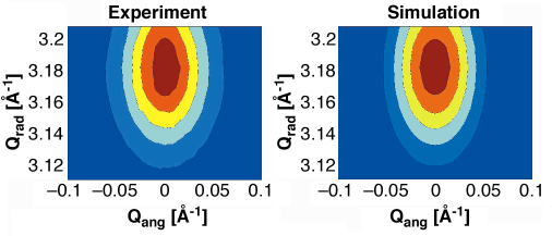
With the input parameter for the size and shape as obtained from AFM and GID, an atomistic simulation of the diffraction pattern was performed. Variable fit parameters were the lateral size of a cylindrical dot and its height-dependent strain evolution. Due to the small size of the dots, this method allows to fit reciprocal space maps in an acceptable calculation time even on an atomistic scale. The measured diffuse intensity distribution is presented in Figure 36 together with the fitted model.
 |
|
Fig. 36: qangular/qradial reciprocal space map at the (220) surface reflection: comparison between experimental results and atomistic simulation. |
In conclusion, nanometric size Ge dots have been grown in epitaxy to the silicon (001) surface. The smaller dots are almost fully strained to the silicon. The bigger dots exhibit a large distribution of the in-plane lattice parameter which indicates a high degree of strain relaxation. Further work is clearly necessary in order to determine the mechanism of the strain relaxation, the chemical composition and the critical diameter (size) of dots before the relaxation phenomenon appears.
References
[1] A. Barski, M. Derivaz, J.L. Rouvière, and D. Buttard, Appl. Phys. Lett. 77, 3541 (2000).
[2] M. Derivaz, P. Noé, J.L. Rouviere, D. Buttard, D. Sotta, P. Gentil and A. Barski, Mat. Sci. and Eng. B 89, 191 (2002).
[3] M. Derivaz, P. Noé, R. Dianoux, A. Barski, T. Schülli, T.H. Metzger, Appl. Phys. Lett. 81, 3843 (2002).
Authors
M. Derivaz (a), P. Noé (a), R. Dianoux (a), A. Barski (a), T. Schulli (b), T.H. Metzger (b).
(a) CEA Grenoble / DRFMC (France)
(b) ESRF
partners


European Synchrotron Radiation Facility - 71, avenue des Martyrs, CS 40220, 38043 Grenoble Cedex 9, France.