- Home
- News
- Spotlight on Science
- Probing strain and...
Probing strain and emission in germanium-alloyed nanocrystals
19-12-2025
A robust multimodal synchrotron-based strategy combining nanoscale XRF, SXDM, XANES, and XEOL was employed to build a correlative picture of local composition, strain, and optical properties in germanium-alloyed tin dioxide nanocrystals. The study leverages the unique capabilities of the ID16B and ID01 beamlines to perform complementary X-ray analyses on individual nanostructures. The findings provide new insights into how germanium incorporation and strain modulate defect chemistry and luminescence, offering a pathway to tailor optical responses in ultrawide-bandgap oxide nanomaterials for advanced optoelectronic applications.
Share
The challenge
Rutile-phase germanium dioxide (GeO2) and its alloys, such as tin–germanium dioxide (Sn1-xGexO2), are promising ultrawide-bandgap semiconductors (4.4–4.7 eV) that combine high carrier mobilities, ambipolar dopability, and excellent thermal conductivity [1,2]. However, GeO2 typically crystallises in the α-quartz or amorphous phases at ambient conditions, limiting access to its rutile form. Alloying with rutile SnO2 provides a route to stabilise this metastable phase, but synthesis remains challenging. Nanostructuring provides a pathway to overcome these constraints by accommodating larger lattice distortions and enabling Ge incorporation well beyond the SnO2 bulk solubility limit, unlocking bandgap engineering and tuneable optoelectronic properties.
A bottom-up methodology previously demonstrated in [3] harnesses single-crystalline Zn2GeO4 nanowires as a growth platform. Exploiting the Plateau–Rayleigh instability, amorphous GeO2 droplets spontaneously form along the nanowires and act as confined nucleation sites in a Sn-rich atmosphere, yielding spatially localised rutile Sn1-xGexO2 nanocrystals. This self-organised process enables precise control over crystallite positioning and composition while maintaining structural coherence with the underlying nanowire. The resulting nanocrystals exhibit well-defined faceting and hold promise for optoelectronic applications.
The experiment
This work investigated how Ge incorporation affects the structural and optical properties of Sn1-xGexO2 nanocrystals grown on Zn2GeO4 nanowires, using a correlative, multimodal approach at the ID01 and ID16B beamlines. Nanoscale X-ray fluorescence (XRF), scanning X-ray diffraction microscopy (SXDM), X-ray absorption near-edge structure (XANES), and X-ray excited optical luminescence (XEOL) enabled mapping of composition, strain, and luminescence at the level of individual crystallites.
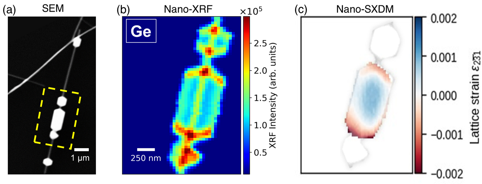
This correlative analysis yielded several key insights into the functional properties of Sn1-xGexO2 nanocrystals. XRF mapping revealed a distinctive “sandwich-like” Ge distribution, with preferential accumulation along the faceted edges of the nanocrystals (Figure 1).
Click figure to enlarge
Fig. 1: (a) Scanning electron microscopy (SEM) image of a representative heterostructure featuring faceted Sn1-xGexO2 crystallites decorating a central Zn2GeO4 nanowire (~100 nm diameter). (b) XRF map showing the spatial distribution of Ge (K-line emission). (c) Spatial distribution of lattice strain epsilon_231, calculated from variations in the interplanar spacing relative to the mean value across the crystallite. The distinct sandwich-like strain pattern reflects compositional heterogeneity associated with Ge-rich and Ge-poor regions shown in (b).
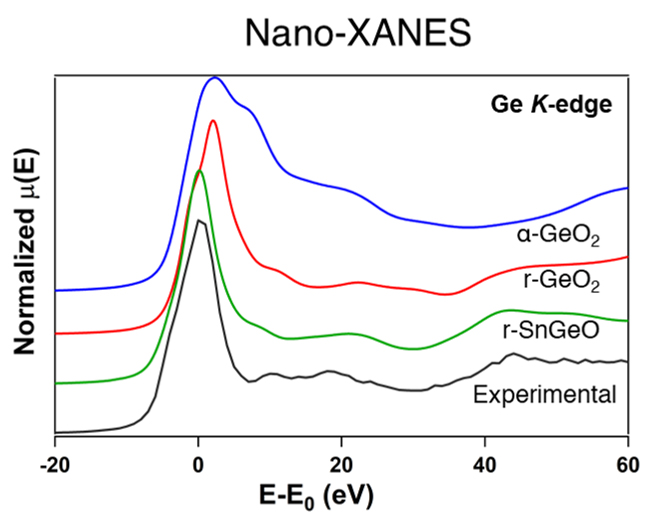
This compositional inhomogeneity coincided with localised strain variations observed via SXDM (Figure 1), particularly near Ge-rich regions and faceting transitions. Despite these internal strain gradients, the rutile lattice remained structurally coherent across all crystallites. Nano-XANES measurements further confirmed substitutional incorporation of Ge atoms into the SnO2 rutile lattice, with no detectable secondary phases present (Figure 2).
Click figure to enlarge
Fig. 2: Experimental XANES spectrum (black line) compared with FDMNES-simulated spectra for α-quartz GeO2 (blue), rutile GeO2 (red), and rutile Sn1-xGexO2 with x=0.18 (green). All spectra are plotted as a function of energy relative to the absorption edge (E – E0, in eV; where E0 is defined as the energy corresponding to the maximum of the first derivative) and are vertically offset for clarity. The strong agreement between the experimental and rutile-phase simulations confirms that Ge is incorporated within a rutile-like coordination environment across the crystallite.
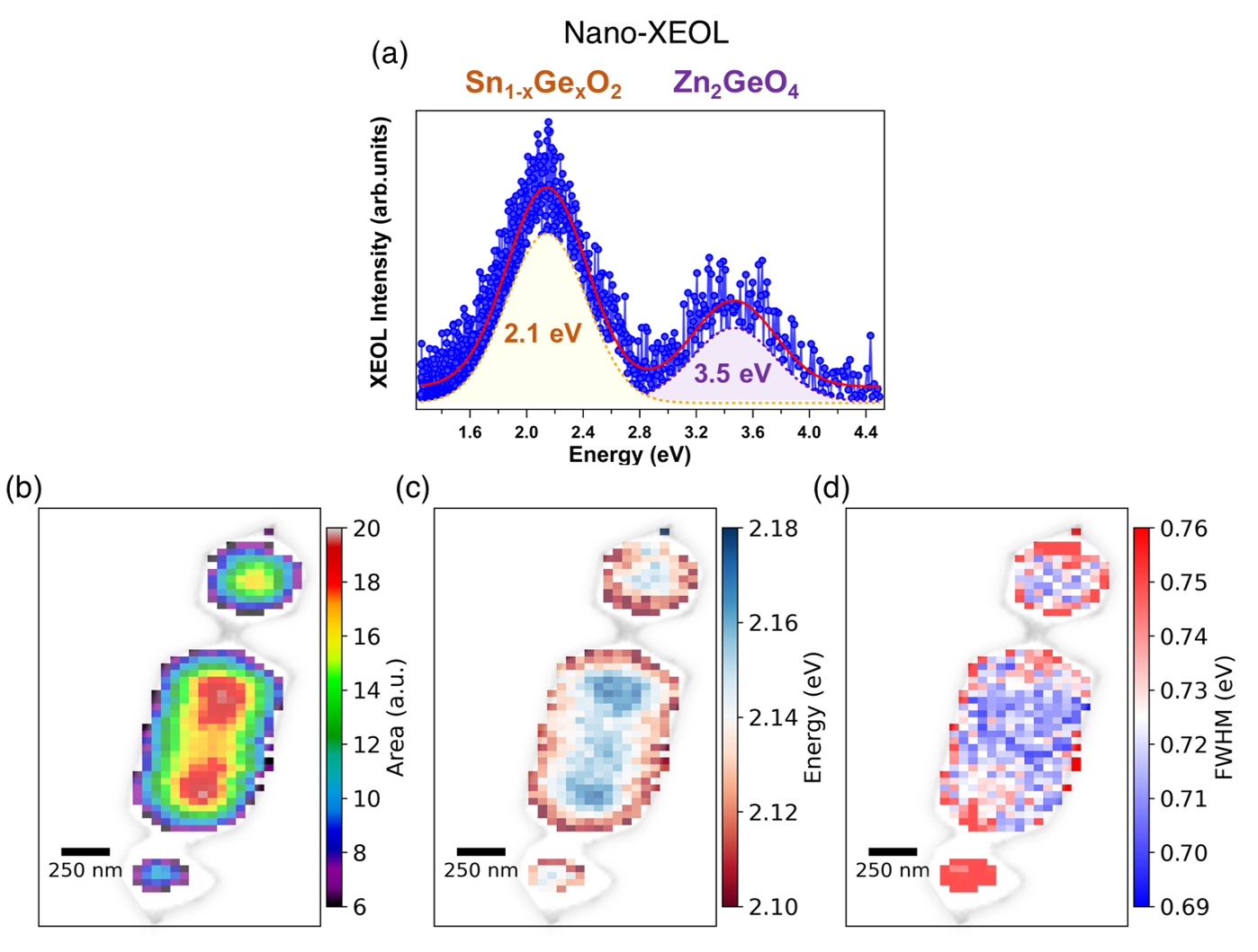
Nano-XEOL spectra revealed broadband visible luminescence (Figure 3), predominantly arising from oxygen-vacancy and surface states. Notably, the emission intensity was significantly enhanced at the Ge-rich edges of the crystallites, linking local structural and compositional variations to optical response.
Click figure to enlarge
Fig. 3: (a) Average XEOL spectrum recorded across the sample. Spatial maps of (b) integrated emission intensity (area under the fitted Gaussian peak), (c) peak energy position, and (d) full width at half maximum (FWHM) of the visible luminescence band within the Sn1-xGexO2 nanocrystals.
Complementary density functional theory (DFT) calculations support these findings by showing that Ge incorporation modifies the bandgap but does not introduce intrinsic mid-gap states. Instead, it reduces the formation energy of oxygen vacancies and alters the distribution of defect states, affecting carrier recombination dynamics. These effects, together with the increased density of surface states at the faceted edges, explain the observed spatial variation in luminescence.
The impact
In summary, this study provides direct insight into how local composition, strain, and defect chemistry are interlinked in Sn1-xGexO2 rutile nanocrystals. The results not only deepen the understanding of Sn1-xGexO2 nanostructures but also point toward new strategies for tailoring their optoelectronic functionalities. More broadly, this work demonstrates the power of synchrotron-based nanoprobes as a unified platform for dissecting complex semiconductor systems with high spatial, structural, and spectral resolution.
Principal publication
Probing Ge-Induced Strain and Emission in Rutile Sn1–xGexO2 Nanocrystals, J. Dolado et al., ACS Appl. Mater. Interfaces 17(48), 65801-65812 (2025); https://doi.org/10.1021/acsami.5c12549
References
[1] H. Takane et al., Phys. Rev. Mater. 6, 084604 (2022).
[2] F. Liu et al., Commun. Mater. 3, 69 (2022).
[3] J. Dolado et al., Cryst. Growth Des. 20, 506-513 (2019).
| About the beamlines: ID01 and ID16B |
| ID01 is a versatile X-ray diffraction and scattering beamline capable of delivering beams as small as 35 nm. It is dedicated to the investigation of a wide range of crystalline materials, from nanostructures to bulk, with the ability to image strain and structure using full-field diffraction imaging, coherent X-ray diffraction methods, and nanodiffraction. Typical samples include microelectronic devices, novel metal-organic solar cells, and battery electrodes. |
| ID16B is a hard X-ray nanoprobe designed for 2D or 3D analysis of heterogeneous materials, combining X-ray fluorescence (XRF), diffraction (XRD), absorption spectroscopy (XAS), excited optical luminescence (XEOL), X-ray beam induced current (XBIC), and phase-contrast imaging. It supports low temperature, in-situ and operando sample environments. ID16B is dedicated to research areas of significant scientific and societal importance, including nanotechnology, Earth and environmental sciences, and biomedical research. |
partners


European Synchrotron Radiation Facility - 71, avenue des Martyrs, CS 40220, 38043 Grenoble Cedex 9, France.