- Home
- A superconducting device drawn by focused X-rays without etching the crystal
A superconducting device drawn by focused X-rays without etching the crystal
We describe the fabrication of a proof-of-concept Josephson device out of a single crystal of a superconducting oxide by means of X-rays nanoprobe irradiation. Our method patterns a superconducting device by selectively removing some of its atoms. This relies on a local change of electrical properties without disrupting the crystal structure and can probably be applied to oxides in general.
In the microelectronics rush towards smaller and faster circuits, the idea of establishing photolithographic processes based on X-rays to take advantage of their very small wavelength (λ ≲ 1 nm) has already been explored, but the problems related to the fabrication of masks with the necessary contrast and small sizes have discouraged further efforts [1]. However, those approaches were based on the traditional scheme of light exposure and etching: a pattern is defined on some organic material, where the X-ray energy induces some difference in the chemical resistance to the developing solution, and then the pattern is transferred to the electronically active material by means of an etching process.
Nowadays, the appearance of oxide electronics is opening new possibilities. Indeed, the discovery of 2D electron liquids at some oxide/oxide interfaces or the fabrication of oxide-based memory cells are positioning oxide technology side by side with silicon technology. However, electrical properties of oxides are very sensitive to the presence of oxygen vacancies in the crystal lattice, and in principle this kind of vacancy can be directly induced by X-rays because of the small mass of oxygen atoms. It should therefore be possible to change the conducting/insulating properties of oxides locally by X-ray irradiation, with no need for mediating organic materials or etching processes. Following our recent encouraging results [2], we tested this idea on the superconducting oxide Bi2Sr2CaCu2O8+δ (Bi-2212), whose typical critical temperature is Tc ≈ 80-90 K.
Bi-2212 can be described as a stack of superconducting crystal planes containing Cu ions, intercalated by insulating planes containing Bi ions. There are two specific features corresponding to this crystal structure: i) the current senses much less resistance when flowing along the Cu planes compared to the normal direction, and ii) in the superconducting state, all of the Cu planes are coupled via the Josephson effect because of the thinness of the Bi insulating layers. Moreover, both the conducting and the superconducting properties depend very strongly on the content of O ions.
 |
|
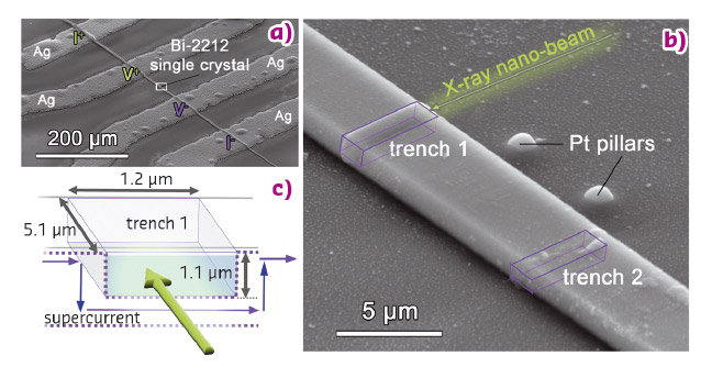
Fig. 34: a) Typical layout of the chip used for device writing. Current and voltage electrodes are labelled as I+, I–, V+ and V–. b) Irradiation geometry used at ID16B to pattern the device in the central part of the chip. Pt pillars are used for alignment purposes only. Superconducting Cu planes are parallel to the substrate. c) Sketch of trench 1, along with the supercurrent path induced by the trench. The green arrow represents the X-ray nanobeam. |
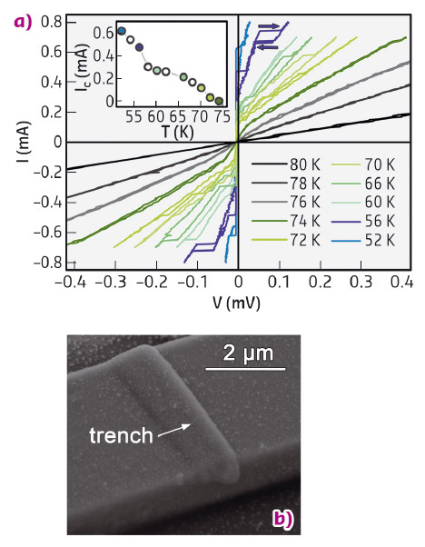
Therefore, we irradiated the Bi-2212 crystals with the 57 × 45 nm2 probe at beamline ID16B, as shown in Figure 34, to pattern two "trench" regions by inducing non-superconducting properties locally. By displacing the "trenches" along the direction of the crystal thickness (trench 1: up, trench 2: down), we tried to force the current along the more difficult direction, i.e. normal to the Cu planes, obtaining a zig-zag path for the current. Experimental evidence of successful patterning is provided by Figure 35a, because the typical Josephson behaviour of these IV curves can be observed only if the current flows along the direction normal to the superconducting Cu planes. Direct SEM observation reveals that the material has not been removed from the "trench" regions (see Figure 35b), and that just some crystal expansion can be detected. Nano-XRD patterns measured in the "trench" regions have also shown that the Bi-2212 crystal structure is preserved, with the appearance of some Bi2O3 that could be compatible with oxygen loss from the crystals.
 |
|
Fig. 35: a) IV curves at different temperatures for the patterned device. Violet arrows highlight the hysteresis between current-increasing and current-decreasing branches, as expected for underdamped Josephson junctions. The inset shows the increase of the critical current Ic with decreasing the temperature, typical of Josephson junctions. b) View of the sample around trench 1. |
These results demonstrate a conceptually new patterning method for oxide electrical devices based on X-rays, with potential advantages in terms of heat dissipation, chemical contamination and high aspect ratio of the devices.
Principal publication and authors
Direct-write X-ray nanopatterning: a proof of concept Josephson device on Bi2Sr2CaCu2O8+δ superconducting oxide, M. Truccato (a), A. Agostino (b), E. Borfecchia (b), L. Mino (c), E. Cara (a), A. Pagliero (a), N. Adhlakha (a), L. Pascale (b), L. Operti (b), E. Enrico, N. De Leo (c), M. Fretto (c), G. Martinez-Criado (d) and C. Lamberti (b,e), Nano Lett. 16, 1669–1674 (2016); doi: 10.1021/acs.nanolett.5b04568.
(a) Department of Physics, Interdepartmental Centre NIS, University of Torino (Italy)
(b) Department of Chemistry, Interdepartmental Centre NIS and INSTM Centro di Riferimento, University of Torino (Italy)
(c) INRIM, National Institute for Metrological Research, Torino (Italy)
(d) ESRF
(e) Southern Federal University, Rostov-on-Don (Russia)
References
[1] R.F. Pease and S.Y. Chou, Proc. IEEE 96, 248 (2008).
[2] A. Pagliero et al., Nano Lett. 14, 1583 (2014).
partners


European Synchrotron Radiation Facility - 71, avenue des Martyrs, CS 40220, 38043 Grenoble Cedex 9, France.