- Home
- Collective action at the nanoscale: witnessing the formation of a 2D superlattice
Collective action at the nanoscale: witnessing the formation of a 2D superlattice
Two-dimensional systems have recently emerged as very promising candidates for future electronic devices. An ordered 2D array of nanocrystals can be created by letting nanocrystals self-assemble on a liquid surface. This new structure shows excellent long range order at the nanocrystal and atomic level. Experiments at beamline ID10 revealed how nanocrystals order themselves and 'click together' to produce beautiful 2D superlattices.
PbSe nanocrystals self-assemble at the liquid/air interface [1,2]. We have studied this phenomenon using multiple techniques: small-angle X-ray scattering (SAXS) - to study the motion of the nanocrystals on the liquid surface - and wide-angle X-ray scattering (WAXS) - to study the orientation and self-assembly of the nanocrystals at the interface. We performed the experiments in grazing incidence mode (GI), which means that the X-ray beam impinges at a very tiny angle of only 0.3° with respect to the liquid/air interface. This made ID10 our beamline of choice as it is specialised in grazing-incidence scattering experiments on liquid surfaces.
 |
|
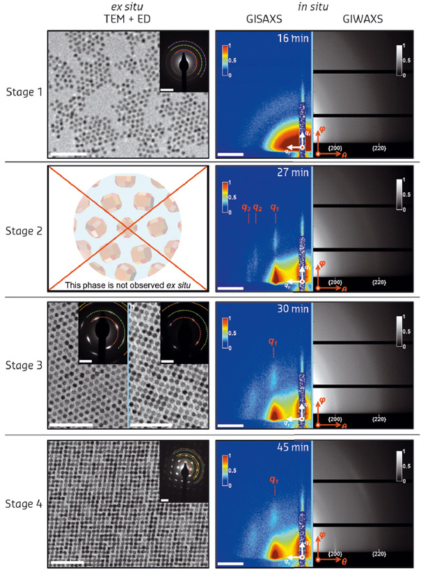
Fig. 108: The different stages during the self-assembly process as monitored by ex situ electron microscopy, electron diffraction and in situ GISAXS/GIWAXS. |
We followed the formation of nanocrystals on two different length scales: on the nanoscale for the movement of the nanocrystals on the liquid surface with GISAXS; and at the atomic length scale with GIWAXS, which probes both the orientation of the nanocrystals with respect to the liquid surface and the crystalline domain size. The results of the in situ X-ray scattering data, together with ex situ electron microscopy and diffraction, are shown in Figure 108.
 |
|
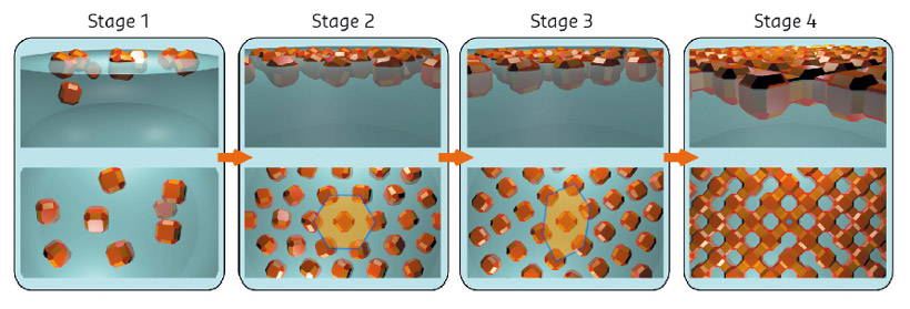
Fig. 109: Model for the self-assembly derived from a combination of in situ X-ray scattering, ex situ electron microscopy and Monte Carlo simulations. |
By combining all the data and performing Monte Carlo simulations, a detailed picture of the self-assembly process was obtained as shown in Figure 109. The nanocrystals are initially dispersed in an apolar solvent which is placed onto a polar liquid substrate. The two solvents do not mix and the nanocrystals are not soluble in the bottom liquid. At stage 1 of the self-assembly process, while the apolar solvent of the nanocrystal solution is evaporating, the increasing concentration of nanocrystals forces them to slowly attach to the interface. At stage 2, most of the apolar solvent has evaporated, and the nanocrystals self-assemble into an energetically favoured dense hexagonal array of nanocrystals (similar to hard-spheres). At stage 3, the hexagonal monolayer starts to deform towards the final square lattice. At stage 4, the nanocrystals are in close proximity and can atomically fuse together by forming crystalline bridges between the nanocrystals.
Synchrotron radiation played a pivotal role in this study. While electron microscopy provided important insights into the structures formed at different stages of the process, it was essentially ex situ. The intermediate structures at stage 2 were only observed using synchrotron techniques as they do not survive upon the sample drying on a grid. Further insights into the mechanism were provided by computer simulations that indicate that there must be an attraction between the nanocrystal {100} facets, caused by either electrostatic or strong Van der Waals interactions.
We have succeeded for the first time in capturing this incredible sequence of phase transitions of nanocrystals during their self-assembly process on a liquid interface. The insights obtained may result in bottom-up routes towards a diversity of 2D electronic or photonic materials based on nanocrystals. The presented procedures will be developed further, such that the self-assembly of nanocrystal colloids can become a feasible alternative to top-down lithography based methods.
Principal publication and authors
In situ study of the formation mechanism of two-dimensional superlattices from PbSe nanocrystals, J.J. Geuchies (a,e), C. van Overbeek (a), W.H. Evers (b,c), B. Goris (d), A. De Backer (d), A.P. Gantapara (f), F.T. Rabouw (a), J. Hilhorst (e), J.L. Peters (a), O. Konovalov (e), A.V. Petukhov (g,h), M. Dijkstra (f), L.D.A. Siebbeles (b), S. Van Aert (d), S. Bals (d) and D. Vanmaekelbergh (a), Nature Materials 15, 1248–1254 (2016); doi: 10.1038/nmat4746.
(a) Condensed Matter and Interfaces, Debye Institute for Nanomaterials Science, Utrecht University (The Netherlands)
(b) Optoelectronic Materials Section, Department of Chemical Engineering, Delft University of Technology (The Netherlands)
(c) Kavli Institute of Nanoscience, Delft University of Technology (The Netherlands)
(d) Electron Microscopy for Materials Science (EMAT), University of Antwerp (Belgium)
(e) ESRF
(f) Soft Condensed Matter, Debye Institute for Nanomaterials Science, Utrecht University (The Netherlands)
(g) Physical and Colloidal Chemistry, Debye Institute for Nanomaterials Science, Utrecht University (The Netherlands)
(h) Laboratory of Physical Chemistry, Department of Chemical Engineering and Chemistry, Eindhoven University of Technology (The Netherlands)
References
[1] W.H. Evers et al., Nano Lett. 13, 2317–2323 (2013).
[2] M.P. Boneschanscher et al., Science 344, 1377-1380 (2014).
partners


European Synchrotron Radiation Facility - 71, avenue des Martyrs, CS 40220, 38043 Grenoble Cedex 9, France.