- Home
- Charge transfer at epitaxial interfaces
Charge transfer at epitaxial interfaces
Differences in the work functions between the constituents of semiconductor interfaces are known to cause charge transfer, band bending and the formation of space charge regions. At interfaces of correlated oxides, the situation can be even more complex since the charge, orbital and spin degrees of freedom can be modified. The materials forming the interface may experience significant modification of their electronic response from the variations in carrier density associated with charge transfer. These modifications occur as a consequence of the very different electronic ground states that coexist in narrow regions of the phase diagrams [1]. We have studied the effect of charge transfer and modified bonding at the interface formed between two Mott-insulators: LaFeO3 (LFO) and Sm2CuO4 (SCO). While LaFeO3 remains insulating and with an antiferromagnetic ground state when moderately doped, Sm2CuO4 becomes metallic and even superconducting upon doping with electrons. In experiments using X-ray absorption spectroscopy with linear polarisation at beamline ID08, we have shown that charge transfer occurs at this interface and as a consequence the heterostructure formed by two insulating materials becomes metallic.
 |
|
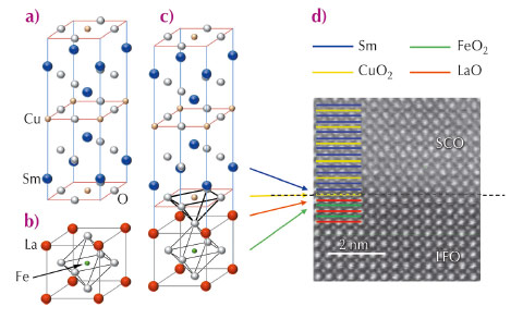
Fig. 107: Crystal structure of (a) Sm2CuO4 (T’-phase), (b) pseudocubic representation of LaFeO3, and (c) interface formed by these compounds. In (c) the interfacial Cu-O pyramid is highlighted. (d) High-resolution scanning transmission electron microscopy image of a [LFO14/SCO4]6 heterostructure. |
We have grown superlattices consisting of six bilayers of 14 unit cells (u.c.) of LFO and N u.c. SCO ([LFO14/SCON]6) on TiO2 terminated SrTiO3 (STO) substrates in a high-pressure pure oxygen sputtering system. Thin films of LFO and SCO were also grown as control samples. The unit cell of SCO and LFO and the schematic of the resulting interface structure are show in Figure 107. The heterostructures are fully strained as confirmed by reciprocal space maps obtained at beamline BM25. The high quality of the interface formed between these oxides was extensively studied by scanning transmission electron microscopy. An atomic-resolution high-angle annular dark-field (ADF) image (also known as Z-contrast) of the interface is shown in Figure 107d. Through analysis of the elemental maps with atomic resolution, we were able to discern the atomic plane stacking, as indicated in the figure by colour bars.
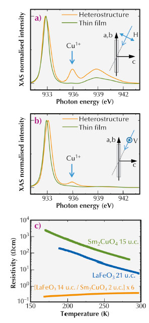
To study the electronic configuration of Cu, we have performed X-ray absorption spectroscopy (XAS) measurements at beamline ID08 with linearly-polarised light. Figure 108 shows the Cu L3 absorption spectrum normalised to the edge jump obtained with horizontal (H) and vertical (V) polarised light, respectively, for a thin film 15 u.c. thick of SCO (green) and a [LFO14/SCO2]x6 superlattice (orange). Schematics of the experimental setup to measure the XAS spectra with H and V-polarised photons, which probe mainly out of plane and in plane orbital states, are shown in the insets. The main peak L3 ≈ 932.8 eV observed in the spectra is associated with transitions from the Cu2+ ground state 2p63d9 to the 2p3/23d10 excited state, where 2p3/2 denotes a 2p3/2 hole.
The remarkable difference between the spectra of both samples is the feature observed at 935.6 eV associated with the presence of Cu1+, clearly visible for the superlattice with H and V polarised light. Nevertheless, in the case of H polarisation the associated peak is more intense indicating the out of plane character of these states. In the case of the superlattice, the Cu atoms in the interfacial CuO2 planes have apical oxygens (Figure 107c), whilst it is known that there are no apical oxygens in bulk SCO. This provides evidence of the existence of a Cu1+ 3d3z2-r2 - apical O 2pz bond resulting from an orbital reconstruction at the interfacial plane. The temperature dependent resistivity of [LFO14/SCO2]6, LFO21 and SCO15 is displayed in Figure 108c. As expected, the two thin films displayed insulating (dR/dT<0) character while the SCO/LFO heterostructure show metallic-like behaviour (dR/dT>0) in the temperature range 300-170 K. Dielectric spectroscopy methods allow the temperature range to be extended to lower values revealing a metal to insulator transition, suggesting an insufficient doping level for superconductivity nucleation.
 |
|
Fig. 108: X-ray absorption spectra obtained with (a) vertical and (b) horizontal polarisation. The spectra corresponds to a [LFO14/SCO2]6 superlattice (orange) and a SCO 15 u.c. thick film (green). (inset) schematics of the of the experimental setup. (c) Resistivity as a function of temperature of samples: [LFO14/SCO2]6, LFO21 and SCO15. |
In summary, we have realised electron doping of SCO by charge transfer in superlattices of SCO/LFO, i.e. between Mott insulators. High resolution electron energy loss spectroscopy measurements and X-ray absorption spectroscopy provided evidence of extra electrons in the Sm2CuO4 d-band. As a consequence of the charge transfer, the heterostructures become metallic as confirmed by a combination of DC transport and dielectric spectroscopy measurements.
Principal publication and authors
F.Y. Bruno (a), R. Schmidt (a), M. Varela (a,b), J. Garcia-Barriocanal (a), A. Rivera-Calzada (a), F.A. Cuellar (a), C. Leon (a), P. Thakur (c), J.C. Cezar (c), N.B. Brookes (c), M. Garcia-Hernandez (d), E. Dagotto (b,e), S.J. Pennycook (b) and J. Santamaria (a), Advanced Materials 25, 1468–1473 (2013).
(a) GFMC. Dpto. Física Aplicada III, Universidad Complutense de Madrid (Spain)
(b) Materials Science and Technology Division, Oak Ridge National Laboratory (USA)
(c) ESRF (d) Instituto de Ciencia de Materiales de Madrid, Consejo Superior de Investigaciones Cientificas, Cantoblanco (Spain)
(e) Department of Physics and Astronomy, University of Tennessee, Knoxville (USA)
References
[1] H.Y. Hwang et al., Nature Mat 11, 103 (2012).
partners


European Synchrotron Radiation Facility - 71, avenue des Martyrs, CS 40220, 38043 Grenoble Cedex 9, France.