- Home
- Users & Science
- Find a beamline
- X-ray nanoprobe
- ID01 - Nano/Micro diffraction imaging
- Science on ID01
- Strain and orientation mapping in thin films and nanostructures
Strain and orientation mapping in thin films and nanostructures
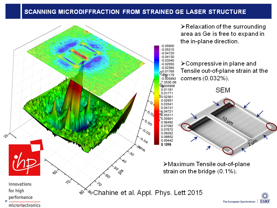
The investigation of structural properties of semiconductor nanostructures or functional materials is widely regarded to be one of the most important issues concerning the development of new technologies on the nanometer scale. Recent efforts on ID01 have led to the development of scanning probe strain microcopy. To this end, smallest x-ray beams (down to 100 nm) were combined with continuous motion of the sample by a piezo-scanner. Performing a rocking curve of the incident angle and using a 2D detector, 3D reciprocal space maps are recorded for every pixel in real space over an area of typically 0.1x0.1 mm2. Fitting the position of the Bragg peak in each reciprocal space map allows the orientation and the lattice parameter distribution to be imaged in real space. The relative strain sensitivity can be below 10-5. The information supplied in such images can not be optained by any other method at comparable precision and field of view. Recent examples from industrial beamtimes have been published:
Zoellner et al., Advanced Materials and Interfaces (2015)
Chahine et al., Appl. Phys. Lett. (2015)
Chahine et al., J. Appl. Cryst. (2014)
![]()
partners


European Synchrotron Radiation Facility - 71, avenue des Martyrs, CS 40220, 38043 Grenoble Cedex 9, France.