- Home
- Artificial graphene made of semiconductor quantum dots
Artificial graphene made of semiconductor quantum dots
Quantum dot superlattices are structures that can be formed through the self-assembly of colloidal semiconductor nanocrystals, which are nanoparticles with size-dependent properties [1]. Many applications have been envisioned for quantum dot superlattices, ranging from solar cells and transistors to LEDs. The properties of such systems depend both on the properties of the constituent particles and on the structure of the superlattice. The novel effects related to the formation of a superstructure remain to be addressed experimentally.
One particular superlattice with very interesting properties is the honeycomb superlattice [2]. It resembles the wonder material graphene, but instead of having carbon atoms at the edges of its honeycomb, it has PbSe or CdSe nanocrystals, which are fused together into a single-crystalline sheet. Theory predicts this material to have properties similar to those of graphene, such as very high charge carrier mobility, which could be conveniently modified by an electric field. In addition, courtesy of its semiconductor building blocks, the electronic properties can be further tuned by the quantum dot composition and size, making the “artificial graphene” very interesting for applications in the electronics industry [3].
Oriented attachment is a specific method for the preparation of such superlattices from the nanocrystal building blocks. In oriented attachment, nanocrystals fuse together through atomically matched bond formation between two specific facets. Precise control of nanocrystal and ligand concentration as well as temperature enabled the synthesis of large area, defect free honeycomb superlattices. The formation of these systems is remarkable, given that several demanding conditions must be fulfilled. The nanocrystal building blocks must be nearly monodisperse in size and shape, and attachment should occur with atomic accuracy, between a geometrically defined subset of nanocrystal facets.
 |
|
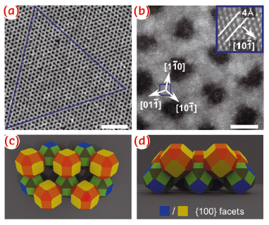
Fig. 121: Single-crystalline PbSe honeycomb structures created by means of oriented attachment. a) HAADF-STEM image of the honeycomb structure (bright on a dark background). The equilateral triangle shows the long-range ordering of the structure. Scale bar, 50 nm. b) High-resolution HAADF-STEM image showing that the ⟨111⟩ NC axes are perpendicular to the honeycomb plane and three of the ⟨110⟩ axes are perpendicular to the (c) and (d) models of the honeycomb structure, with truncated cubes as nanocrystals. The two inequivalent sites in the honeycomb lattice are indicated by yellow/red and blue/green NCs. c) and d) are the top and side view of the octahedral structure, respectively. |
The nanocrystal building blocks have the shape of a truncated cube, approaching that of a rhombicuboctahedron, implying that the nanocrystals are terminated with {100}, {110} and {111} facets. Characterising the honeycomb superlattice with high-angle annular dark field (HAADF) scanning transmission electron microscopy (STEM) combined with electron diffraction reveals that the <111> axis of the nanocrystals is perpendicular to the substrate and that the structure is single crystalline, having all nanocrystals aligned similarly (Figure 121a,b). There are three models which fulfil this condition: a trigonal model, where the nanocrystals attach via {110} facets, a tetrahedral model where they attach via {111} facets and an octahedral model where they attach via {100} facets (see Figure 121c,d). These models appear similar from the top, but have a very different 3-dimensional structure. The trigonal structure is flat, exactly like graphene, whereas the tetrahedral and octahedral structures are buckled comparable to the silicene structure.
The HAADF-STEM images combined with the electron diffraction show that the <110> axes are perpendicular to the superstructure bonds, ruling out the possibility of the trigonal structure (where the <110> axes are parallel to the nanocrystal bonds). In addition, these images show increased scattering strength on the nanocrystal bonds, indicating a larger-than-average thickness of the structure at these positions which originate from the out-of-plane bonding of the honeycomb structure. Scanning tunnelling microscopy (STM) measurements showed that the honeycomb structure is indeed buckled. However in STM, the topography is a complicated convolution of the superlattice topography and the tip shape, so no quantitative height data could be extracted. A next-nearest neighbour distance of nanocrystals at the same height could reliably be extracted, which on average is 8.5 ± 0.8 nm.
 |
|
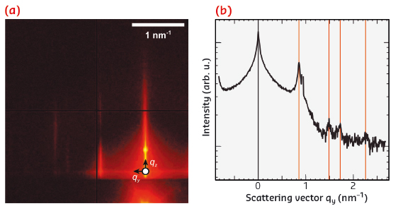
Fig. 122: a) GISAXS pattern of a honeycomb structure on top of a Si(100) substrate obtained at ID01. b) Line trace in the horizontal direction indicated in (a). Red lines mark diffraction peaks with relative positions of 1 : √3 : 2 : √7 arising from the hexagonal symmetry of the honeycomb lattice. |
To further study the long-range order, grazing incidence small-angle X-ray scattering (GISAXS) experiments were performed at ID01 (Figure 122a,b). The scattering pattern shows diffraction rods arising from the hexagonal symmetry of the honeycomb structure, with the expected relative positions of 1 : √3 : 2 : √7. The extracted hole-hole distance of the honeycomb structure, corresponding to the next-nearest neighbour (NNN) distance, is 8.5 nm, which is in agreement with the STM measurements.
To distinguish between the tetrahedral and octahedral model, electron tomography was performed. Slices through the reconstructed tomogram perpendicular to the substrate indicate that the nanocrystals in the honeycomb unit cell are located on different heights. Subsequently, automated particle detection was performed on a region of interest to extract important parameters, such as bond angle, bond length and NNN bond length. The obtained bond length of 95° ± 5° shows that the honeycomb structure is of the octahedral type, with bonds between {100} facets. The bond length was found to be 13% larger than the original nanocrystal diameter, indicating neck formation between the nanoparticles in the superlattice.
It has been predicted that honeycomb semiconductors of zinc blend compounds (such as CdSe) show a truly new electronic band structure. The PbSe honeycomb structure is changed into CdSe via a cation exchange reaction, which has been confirmed by means of energy dispersive X-ray spectroscopy. Combining this with HAADF-STEM and electron diffraction showed that the Se anion lattice is preserved with respect to the honeycomb periodicity.
These results show that the honeycomb lattice, which is buckled and of octahedral symmetry, can be made on a liquid surface, and can subsequently be transformed into a material of interest via cation exchange. A next step in this research will be the in situ measurements of the formation of this remarkable type of crystal.
Principal publication and authors
M.P. Boneschanscher (a), W.H. Evers (b), J.J. Geuchies (a), T. Altantzis (c), B.Goris (c), F.T. Rabouw (a), S.A.P. Van Rossum (a), H.S.J. van der Zant (b), L.D.A. Siebbeles (b), G. Van Tendeloo (c), I. Swart (a), J. Hilhorst (d), A.V. Petukhov (a), S. Bals (c) and D. Vanmaekelbergh (a), Science 344, 1377-1380 (2014).
(a) Debye Institute for Nanomaterials Science, Utrecht University (The Netherlands)
(b) Opto-electronic Materials, Kavli Institute, Delft University of Technology (The Netherlands)
(c) Electron Microscopy for Materials Science (EMAT), University of Antwerp (Belgium)
(d) ESRF
References
[1] W.H. Evers et al., Nano Lett. 13, 2317 (2013).
[2] M.P. Boneschanscher et al., Science 344, 1377 (2014).
[3] E. Kalesaki et. al., Phys. Rev. X 4, 011010 (2014).
partners


European Synchrotron Radiation Facility - 71, avenue des Martyrs, CS 40220, 38043 Grenoble Cedex 9, France.