- Home
- Users & Science
- Scientific Documentation
- ESRF Highlights
- ESRF Highlights 2012
- Structure of materials
- Nanoscale structural distortion in SiGe quantum-electronic heterostructures
Nanoscale structural distortion in SiGe quantum-electronic heterostructures
Semiconductor quantum electronic devices provide the opportunity to manipulate individual quantum states of electrons, and thus promise to extend microelectronics into an entirely new regime. One promising route to forming these quantum structures using the ubiquitous and highly developed processing technology associated with silicon-based microelectronics is to create coupled quantum dots in which electrons are trapped in a thin silicon quantum well layer within a stack of layers of an alloy of silicon and germanium. As in conventional semiconductor devices, the properties of quantum mechanical devices based on the two-dimensional electron gas within the silicon quantum wells depend very strongly on the local atomic-scale structure, and on the changes in the structure induced by the creation of the devices. The role of specific structural defects, including atomic steps and other local sources of distortion, has been predicted theoretically and observed by electrical measurements [1,2], but has been difficult to probe in structural studies. It has been particularly challenging to understand the shape and distortion of the silicon quantum well layer at length scales similar to the size of the confined electron wavefunction.
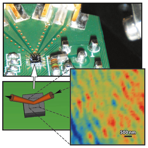
X-ray nanodiffraction allows structural information to be obtained at the length scale relevant to devices within the silicon quantum well. Nanodiffraction studies at beamline ID01 demonstrate that the relevant structural parameters of these layers can be probed using the tightly-focused X-ray beam produced by a Fresnel zone plate. The diffraction experiments (see Figure 109) probe the buried silicon quantum well layer within integrated quantum dots without destructive sample preparation. The nanodiffraction results show that the structure of the silicon quantum well is influenced both by the fundamental processes of epitaxial growth in the silicon/silicon germanium materials systems and by the subsequent lithographic processing required to produce quantum dots.
 |
|
Fig. 109: X-ray nanodiffraction map of the waviness in a 10 nm-thick buried Si quantum well. Si quantum wells in a Si/SiGe heterostructure are characterised using a tightly-focused X-ray beam, without destructive sample preparation. Structural effects at the 100-nm length scale arising from local variations in the quantum well thickness are apparent in the total intensity of the 004 X-ray reflection of the quantum well. |
A key feature of the design of the silicon quantum well is the introduction of a large biaxial tensile strain to modify the band structure within the well. In nanodiffraction studies, this strain allows X-ray reflections from the silicon quantum well to be easily distinguished from the reflections arising from the silicon substrate. In addition, the silicon quantum well has smooth interfaces, which lead to rods of intensity in reciprocal space. Maps of the intensity and angular location of these rods as a function of the position of the X-ray nanobeam provide local information about the thickness and orientation of the silicon quantum well layer. The intensity of the rod extending from the 004 X-ray reflection of the Si quantum well (inset in Figure 109) exhibits variations at the 100 nm length scale that result from local differences in the thickness of the quantum well layer. The intensity exhibits local variations of several percent, a magnitude that is consistent with what would be expected due to unit-cell-scale variations in the thickness of the quantum well. In addition to these local differences in thickness, the local orientation of the atomic planes within the quantum well varies due to the randomness associated with the underpinning silicon-germanium layers of the heterostructure. These orientation variations lead to a lateral variation of the strain in the quantum well over distances of hundreds of nanometres to 1 μm, modifying the potential well confining electrons. Precise structural information allows theoretical studies of the effects of structural features on quantum electronic properties to be tested and will enable the creation of optimised devices.
Principal publication and authors
P.G. Evans (a,b), D.E. Savage (a), C.B. Simmons (a), M.G. Lagally (a), S.N. Coppersmith (a), M.A. Eriksson (a) and T.U. Schulli (b), Adv. Mater. 24, 5217 (2012).
(a) University of Wisconsin, Madison (USA)
(b) ESRF
References
[1] M. Friesen, S. Chutia, C. Tahan and S.N. Coppersmith, Phys. Rev. B 75, 115318 (2007).
[2] L.M. McGuire, M. Friesen, K.A. Slinker, S.N. Coppersmith and M.A. Eriksson, New J. Phys. 12, 033039 (2010).
partners


European Synchrotron Radiation Facility - 71, avenue des Martyrs, CS 40220, 38043 Grenoble Cedex 9, France.