- Home
- Local environment of Gd in GaN
Local environment of Gd in GaN
Recently, Teraguchi et al. [1] observed a Curie temperature larger than 400 K in Ga0.94Gd0.06N. Additionally, Dhar et al. [2] reported an extraordinarily large magnetic moment of Gd in weakly Gd doped GaN layers as well as ferromagnetism above room temperature. Despite the great potential, there are some controversial results on the ferromagnetic interactions in Ga1–xGdxN. Some findings suggest that the crucial mechanism is either the electric polarisation of the hexagonal GaN, or a strong long-range interaction between Gd atoms and certain defects. On the other hand, Gd might be inducing a magnetic moment in Ga and/or N interstitials were being detected; others have attributed the stabilisation of ferromagnetism to nitrogen or gallium vacancies. Moreover, according to a recent theoretical study [3], Ga vacancies are the most effective source of localised holes necessary for a strong ferromagnetic p-d exchange coupling in GaGdN. In addition, several reports have not detected the formation of any secondary phases in GaN, whereas in Gd implanted GaN the presence of precipitates of Gd3Ga2, GdN, and Gd has been observed with high saturation magnetisation. [4] Therefore, the role of Gd on the defect formation, local atomic site configuration, and/or phase separation in GaN is of key importance.
We have studied the incorporation of Gd on 0.5 mm thick GaN films grown by molecular beam epitaxy (concentrations ranging from 1.14 x 10¹⁷ to 1.18 x 1019 cm–3). All GaGdN layers are ferromagnetic at room temperature, as measured by superconducting quantum interference device magnetometry (SQUID). X-ray absorption near edge structure (XANES) and scanning X-ray fluorescence (XRF) measurements were carried out at the microprobe at ID22. It has been argued that high-temperature ferromagnetism in magnetically doped nitrides results from nanoscale regions containing a high concentration of the magnetic constituents. However, at the length scale of the beam size (1.5 x 3.5 µm2), uniform patterns with no intensity changes (< 0.02%) were observed, showing a homogeneous distribution of Ga and Gd. Whereas the expected impurity aggregation effects are observed in heavily rare earth doped GaN, our results suggest no tendency to agglomerate at those low Gd levels.
 |
|
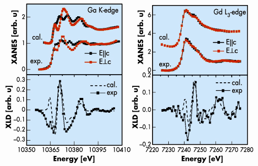
Fig. 139: XANES and XLD signals recorded at the Gd L3 and Ga K edges from the GaN (0.027% Gd). |
The comparison of the X-ray linear dichroism (XLD) of the XANES at the Gd L3 and Ga K edges supports the tetrahedral 6d3+ site distributions in the highest Gd doped GaN (0.027%). Figure 139 shows the XANES recorded with the electrical field vector parallel and perpendicular to the c axis of the GaGdN as well as the respective XLD signal, reflecting directly the anisotropy of the unoccupied density of states of the 5d and 4p shells of the Gd and Ga atoms. The simulations of the XLD performed with FEFF8 code were rescaled with respect to the experimental ones. The Gd L3 edge XLD signal is similar to the one observed at the Ga K edge but with smaller amplitudes. The results show a strong anisotropy exhibiting the signature of the hexagonal GaN. There is no remarkable damping effect revealing a strong influence of the Gd impurities in any preferential crystallographic direction. For other possible Gd site occupation rather than substitutional, the spectral shape and amplitude of XLD signal is drastically different [5].
In summary, structural analysis based on XANES and XLD revealed Gd ions in a predominantly trivalent state with tetrahedral coordination, occupying Ga sites in the wurtzite structure. In addition, EXAFS collections around Ga atoms have shown no local atomic distortion as a function of Gd fraction providing direct evidence for the highly short range structural order. Although the presence of very small amounts cannot be completely excluded, within the sensitivity of our experimental techniques, neither secondary phases nor Ga vacancies were observed.
Principal publication and authors
G. Martínez-Criado (a), O. Sancho-Juan (b), N. Garro (b), J.A. Sans (a), A. Cantarero (b), J. Susini (a), M. Roever (c), D.-D. Mai (c), A. Bedoya-Pinto (c), J. Malindretos (c) and A. Rizzi (c), Appl. Phys Lett. 93, 021916-1-3 (2008).
(a) ESRF
(b) ICMUV, 46071-València (Spain)
(c) VISel, D-37077 Göttingen (Germany)
References
[1] N. Teraguchi, A. Suzuki, Y. Nanishi, Y.K. Zhou, M. Hashimoto, and H. Asahi, Solid State Commun. 122, 651 (2002).
[2] S. Dhar, O. Brandt, M. Ramsteiner, V.F. Sapega, and K.H. Ploog, Phys. Rev. Lett. 94, 037205 (2005).
[3] L. Liu, P.Y. Yu, Z. Ma, and S.S. Mao, Phys. Rev. Lett. 100, 127203 (2008).
[4] S.Y. Han, J. Hite, G.T. Thaler, R.M. Frazier, C.R. Abernathy, S.J. Pearton, H.K. Choi, W.O. Lee, Y. D. Park, J.M. Zavada, and R. Gwilliam, Appl. Phys. Lett. 88, 042102 (2006).
[5] A. Ney, T. Kammermeier, E. Manuel, V. Ney, V.S. Dhar, K.H. Ploog, F. Wilhelm, and A. Rogalev, Appl. Phys. Lett. 90, 252515 (2007).
partners


European Synchrotron Radiation Facility - 71, avenue des Martyrs, CS 40220, 38043 Grenoble Cedex 9, France.