- Home
- High domain wall velocity induced by low current densities in spin valve nanostripes
High domain wall velocity induced by low current densities in spin valve nanostripes
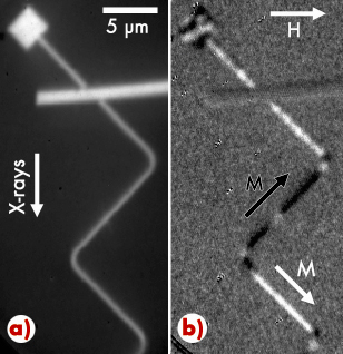
Moving magnetic domain walls in nanostripes using electric currents via spin-torque effects rather than magnetic field pulses is one of the recent exciting developments in spintronics [1]. Achieving reproducible domain wall movements with low current densities and high domain wall velocities is the main challenge in this field of science. The critical current densities necessary to move a domain wall in single layer FeNi nanostripes are of the order of 1012 A/m2 with zero magnetic field, while velocities spread from some m/s up to about 100 m/s. These current densities are too high for applications. Lower current density values have been found for spin-valve-based nanostripes. Our work shows the first direct evidence that in such materials very high domain wall velocities (exceeding 170 m/s) at zero field can be obtained for current densities much lower than for FeNi. We have used photoemission electron microscopy (PEEM) combined with X-ray magnetic circular dichroism (XMCD) to measure domain wall movements in the permalloy layer of 400 nm wide FeNi(5 nm)/Cu(8 nm)/Co(7 nm)/CoO(3 nm) nanostripes (Figure 108a). The measurements were performed at beamline ID08. The X-ray energy was tuned to the Ni L3 absorption edge to probe the FeNi magnetic structure.
The remanent magnetic state obtained for a 90° angle zigzag nanostripe after application of an in-plane external field perpendicular to the zigzag long axis, is shown in Figure 108b. Magnetic domains with magnetisation pointing downwards/upwards along the nanostripe (white/black contrast) are separated by domain walls. A black-white-black-white contrast is visible at the bends. This contrast is due to the fact that the stray field generated by head-to-head or tail-to-tail domain walls in the bends of the Co layer induces a local antiparallel alignment between Co and FeNi layers in the vicinity of the Co domain wall [2]. We found that these magnetostatic interactions prevent domain wall motion across the bends, but do not hinder domain wall motion away from the bends.
 |
|
Fig. 108: Topographic a) and magnetic b) PEEM images of a spin-valve-like nanostripe with a zigzag angle of 90°, taken at the Ni L3-edge. The sample is magnetised with a static in-plane magnetic field, as indicated by the white arrow. In (b), white (black) contrast corresponds to FeNi domains with a magnetisation component parallel (antiparallel) to the incoming X-ray direction. |
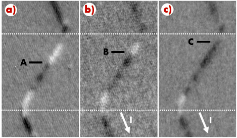
Figure 109 shows current-induced domain wall motion in a stripe with zigzag angles of 120°. The initial magnetic state shown in Figure 109a was obtained reproducibly in situ by applying an ultrafast magnetic field pulse. Figure 109b shows the domain structure obtained after applying one 100 ns long current pulse with amplitude +2 mA. This current pulse causes a displacement of the domain wall initially in position A, towards position B in the images.
Note that the other domain walls present in the nanostripe are not affected by the current. This shows that the pinning strength can be very different at different sample positions.
A second current pulse with the same amplitude and length moves the same domain wall from B to C (Figure 109c). The two current pulses induce a domain wall movement of (1.7 ± 0.2) µm and (1.9 ± 0.2) µm respectively, resulting in domain wall velocities of the order of 20 m/s. When the current is increased to 5 mA the measured DW velocities are of the order of 170 m/s. The current density corresponding to this current value is 5 x 10¹¹ A/m2, if we consider a uniform current distribution through the trilayer stack. These domain wall velocities are well above literature values for single FeNi layers, for current densities that are at least a factor two smaller.
 |
|
Fig. 109: XMCD-PEEM images of the FeNi layer in a zigzag nanostripe with angle of 120°; a) initial state with domain wall in position A; b) after application of one 100 ns current pulse of +2 mA, which shifts the domain wall to B; c) after application of a second 100 ns current pulse of +2 mA, which shifts the domain wall to C. |
Currently used spin-torque phenomenological models do not allow such large domain wall velocities to be explained, and other spin transfer mechanisms should therefore be considered. In our spin-valve structures part of the incident spin flux in the FeNi layer is transformed, in the region around the domain wall, into spin accumulation in the Cu and Co layers. Spin accumulation in the Cu spacer below the domain wall induces a vertical spin current that flows into the domain wall and exerts an additional torque on the domain wall. Our results suggest that the yield of this additional vertical spin transfer channel is much higher than the yield of the in-plane spin transfer channel, as predicted recently by micromagnetic simulations on similar nanostructures containing a single domain wall.
Our direct observation of very fast current-induced domain wall motion confirms the potential application of spin-valve systems to domain wall-based magnetic memories and logic devices.
Principal publication and authors
S. Pizzini (a), J. Vogel (a), V. Uhlir (a), E. Bonet (a), N. Rougemaille (a), S. Laribi (b), F. Petroff (b), V. Cros (b), E. Jiménez (c), J. Camarero (c), C. Ulysse (d), G. Faini (d), C. Tieg (e), Applied Physics Express, accepted.
(a) Institut Néel, CNRS and UJF, Grenoble (France)
(b) Unité Mixte de Physique CNRS/Thales and Université Paris Sud 11, Palaiseau (France)
(c) Dpto. Fisica de la Materia Condensada, Universidad Autonoma de Madrid and IMDEA-NANO, Madrid (Spain)
(d) CNRS, PhyNano Team, Laboratoire de Photonique et de Nanostructures, Marcoussis (France)
(e) ESRF
References
[1] S. Parkin, M. Hayashi, L. Thomas, Science 320, 190 (2008).
[2] J. Vogel, S. Cherifi, S. Pizzini, F. Romanens, J. Camarero, F. Petroff, S. Heun, and A. Locatelli, J. Phys.: Condens. Matt. 19, 476204 (2007).
partners


European Synchrotron Radiation Facility - 71, avenue des Martyrs, CS 40220, 38043 Grenoble Cedex 9, France.