- Home
- Users & Science
- Scientific Documentation
- ESRF Highlights
- ESRF Highlights 2003
- Surface and Interface Science
- InAs Quantum Sticks: Determination of Strain, Size and Composition
InAs Quantum Sticks: Determination of Strain, Size and Composition
The new generation of electronic and optoelectronic integrated circuits are nowadays based on semiconductor nanostructures. InAs quantum wires and quantum dots can be employed as active region materials of lasers and LEDs. To be suitable for devices, the nanostructures are encapsulated with InP or embedded in a superlattice. They must be homogeneous in size, shape and composition, to provide well-defined emission wavelengths. The knowledge of strain field, chemical gradients, chemical mixing at the interface, is therefore of a great importance.
We report on an X-ray study of InAs stick-like islands, quantum sticks, embedded in InP with a 10 nm thick cap layer. These samples are obtained by optimisation of the MBE growth parameters to minimise the As/P exchange and reduce the height dispersion of the InAs islands [1]. The strain of buried nanostructures is mainly related to their composition. It also depends on their size, morphology, and cap layer thickness. Tuning the X-ray energy near an absorption edge of atoms that belong to the nanostructures is a way to modify their scattering power and to enhance the chemical sensitivity of diffraction. We report on a general method that takes advantage of the full capability of anomalous diffraction and can be applied to the very interesting and challenging case of small size embedded nanostructures.
 |
|
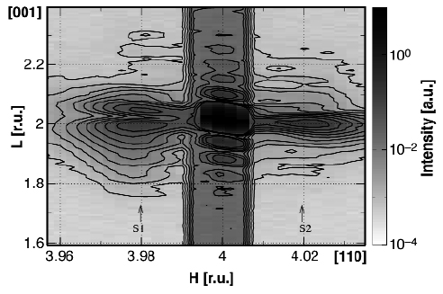
Fig. 91: Experimental diffraction map around the weak InP (442) reflection recorded at 11.840 keV in grazing- incidence geometry; S1 and S2 are correlation satellites due to the stick's short range periodicity along the [110] direction. |
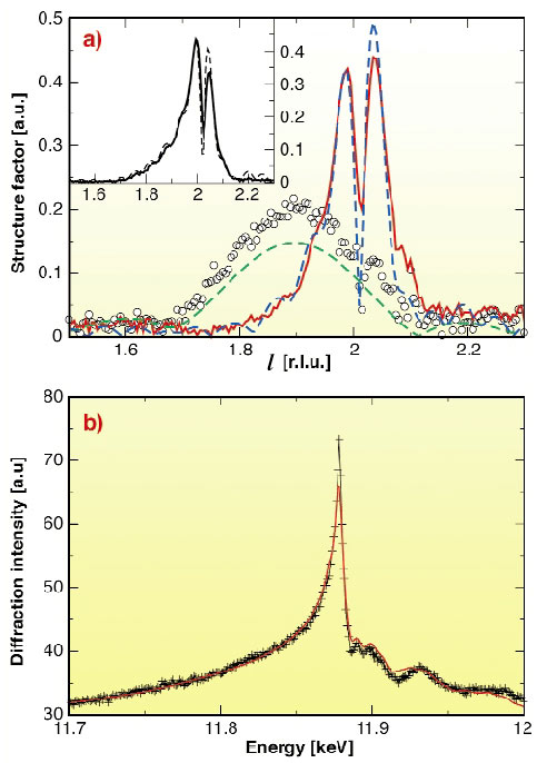
Grazing-incidence anomalous diffraction at the As K-edge (11.867 keV) was performed at the French Collaborative Research Group beamlines BM32 and BM2. Figure 91 shows the diffraction intensity map in the vicinity of the (442) InP substrate reflection, recorded at 11.840 keV and at a grazing-incidence angle near to the critical angle. The spread of scattering in the [110] direction is due to both short range correlation and lattice strain in the real space. Whereas, in the [001] direction, this is due to the sharp strain evolution at the interface. We performed l-scans (h = k = 3.98) accross the satellite S1, at several energies close to the As K-edge. Figure 92a shows the experimental modulus of FA, the As atoms partial structure factor, and FT, the structure factor of all atoms (Thomson scattering). As deduced from the Full Width at Half Maximum (FWHM) of FA, the quantum sticks height average value is about 2.54 nm. In order to determine the quantum sticks composition and the local strain accommodation, Grazing-incidence Diffraction Anomalous Fine Structure (DAFS) spectrum was measured at the maximum of FA (h = k = 3.98 and l = 1.9) at the As K-edge. Figure 92b shows the experimental DAFS spectrum, that is perfectly reproduced with pure InAs quantum sticks.
Finite Difference Method (FDM) simulations were performed to map the strain produced by InAs quantum sticks embedded in InP and compare its Fourier transform to experimental diffraction intensity maps. Figure 92a shows the best calculated curves of FA and FT, obtained by optimising the height and width of the wires, as well as As/P intermixing at the InAs/InP interface. The FDM simulation reproduces well the relative positions of FA and FT, with a strain of about 6.1% with respect to InP substrate in the inner part of the wire. The experimental curves FA and FT are compatible with a weak As/P intermixing at the InP interface, that would spread over one monolayer.
 |
|
Fig. 92: (a) Experimental FT (solid line) and FA (ooo) modulus as a function of the reciprocal lattice unit l at h = k = 3.98 (across the satellite S1). FA is the structure factor of all anomalous atoms, i.e. As atoms only. Also shown are best simulation curves (dashed line) obtained with a finite difference model made of pure InAs quantum sticks with a truncated triangle side profile. Inset shows the experimental (solid line) and simulated (dashed line) square root of the diffraction intensity at 11.867keV; at this energy, anomalous diffraction is maximised. (b) GIDAFS spectrum ( + ) recorded, at the As K-edge, at the maximum of the FA profile (l = 1.9) and the best fit curve obtained with pure InAs structure (solid line). |
In conclusion, we have shown that anomalous diffraction can be used to extract the structure factor of small size InAs nanostructures embedded in InP matrix. This study is a first step towards a 2D and 3D analysis of anomalous diffraction maps and grazing-incidence DAFS data to recover the strain, size, shape and composition of embedded nanostructures.
References
[1] M. Gendry, C. Monat, J. Brault, P. Regreny, G. Hollinger, B. Salem, G. Guillot, T. Benyattou, T.C. Bru-Chevallier, G. Bremond, O. Marty. J. Appl. Phys. (2003).
Principal Publication and Authors
A. Letoublon (a), V. Favre-Nicolin (a), H. Renevier (a), M.G. Proietti (b), C. Monat (c), M. Gendry (c) O. Marty (d), C. Priester (e), submitted to Phys. Rev. Lett. (2003), cond-mat/0309522.
(a) CEA, Grenoble (France)
(b) CSIC-Universidad de Zaragoza (Spain)
(c) LEOM, UMR-CNRS 5512, Ecole Centrale de Lyon (France)
(d) LENAC, Université Lyon I (France)
(e) Institut d'Electronique, de Microélectronique et de Nanotechnologie, Villeneuve d'Ascq (France)
partners


European Synchrotron Radiation Facility - 71, avenue des Martyrs, CS 40220, 38043 Grenoble Cedex 9, France.