- Home
- Users & Science
- Scientific Documentation
- ESRF Highlights
- ESRF Highlights 2001
- Applied and Industrial Research
- How Synchrotron Light can Help Develop Faster Computers
How Synchrotron Light can Help Develop Faster Computers
The continuing drive for the production of faster electronic devices requires technological developments in all stages of chip manufacture. The improvement of the manufacturing process can only be effective when appropriate metrology techniques are available for monitoring during both the development and production phase. A key parameter for yield and reliability management in the fabrication cycle is contamination control and consequently a wide variety of analytical techniques are employed to monitor the cleanliness of both the manufacturing processes and the raw materials involved. One of the most demanding structures in silicon-based transistor technology is the insulating SiO2 gate oxide which separates the transistor gate contact from the Si channel for current flow between the source and drain electrodes. The trend towards a reduction in the lateral dimensions of transistor structures is necessarily accompanied by a reduction in the thicknesses of this film the current technology uses insulating film thicknesses of as little as 25 atoms. Metallic contaminant atoms in this oxide film can "poison" its insulating properties causing short circuits and hence device failure.
Faced with these difficulties, device manufacturers have developed sophisticated procedures to ensure the cleanliness of the wafer surfaces prior to oxide formation and other processing steps. Among the methods employed to evaluate the levels of surface contamination, total-reflection X-ray fluorescence (TXRF) is widely used. TXRF is a non-destructive, quantitative, surface chemical analysis technique based upon the detection of characteristic X-ray fluorescence emission from elements excited by a primary X-ray beam incident at grazing angles on a sample. In common with most other X-ray fluorescence techniques, the measurement consists of the acquisition of an X-ray spectrum (counts vs energy) using an energy-dispersive detector. The energies of the observed peaks allow an identification of the elements present (each element giving rise to a discrete and well-defined fluorescence signature). The intensities of the observed peaks are related to the concentrations of the elements in the X-ray beam excited region. TXRF uses the phenomenon that a flat smooth substrate (such as a typical silicon wafer) will totally reflect an X-ray beam which impinges upon the surface at a sufficiently small, "critical" angle. Under these conditions the beam penetration into the substrate is reduced to a surface layer of a few tens of Ångström thickness. As a consequence, the characteristic fluorescence contribution from the substrate is minimised and the sensitivity to surface localised elements is greatly enhanced.
Although TXRF is extensively used as an in-fab analysis tool for wafer quality control and characterisation, the limited beam intensity of conventional tube or rotating anode based X-ray sources restricts the sensitivity of the measurements. By coupling the TXRF technique with a high brightness synchrotron X-ray source, the combination of increased beam flux, energy tunability and reduced background allows an improvement in the attainable detection limits which satisfies the metrology needs for the next generation of semiconductor devices. Figure 157 shows a TXRF spectrum acquired from a 200 mm ultra-clean silicon substrate at the ID27 TXRF facility which provides an analytical service for contamination control for industrial users. The detected contamination levels are of the order of 108 atoms/cm2 and the spectra indicate a minimum detection limit for the transition elements of a few several 107 atoms/cm2: equivalent to a number of contaminant atoms of a few hundredths of a millionth of a silicon monolayer!
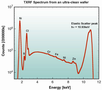 |
Fig. 157: SR-TXRF spectrum from a ultra-clean wafer used as across calibration test between SSRL and ESRF TXRF facilities. The Cr, Fe and Ni contaminants are in the order of few 108 at/cm2 and the lower limit of a detection in 107 at/cm2 scale. |
Authors
R. Barrett and F. Comin
ESRF
partners


European Synchrotron Radiation Facility - 71, avenue des Martyrs, CS 40220, 38043 Grenoble Cedex 9, France.