- Home
- News
- Spotlight on Science
- Why hexagonal boron...
Why hexagonal boron nitride grows differently on liquid and solid copper
04-09-2026
Liquid metal catalysts transformed the growth of graphene towards larger, higher-quality crystals, and were expected to do the same for other 2D materials. Operando grazing-incidence X-ray diffraction and X-ray reflectivity at beamline ID10-SURF reveal how hexagonal boron nitride grows on liquid and solid copper. Liquid copper drives multilayer growth, while solid, single-crystal copper yields epitaxially aligned monolayers. The distinction lies in the interaction strength between the film and the metal, measured at sub-ångström precision during growth.
Share
The challenge
Two-dimensional hexagonal boron nitride (hBN) is the insulating counterpart to graphene, and is the material of choice for separating and protecting layers in van der Waals nanoelectronics. This role depends on the film being a single layer thick and uniform across the wafer. Hence, hBN’s wider use is held back by the difficulty of growing large, uniform, high-quality films, and that difficulty itself stems from an incomplete picture of how hBN actually grows.
One of the most effective routes to synthesise 2D materials is chemical vapour deposition (CVD), carried out on a catalyst substrate. Liquid metal catalysts such as molten copper are especially attractive since a liquid surface is atomically smooth, such that steps and grain boundaries which disrupt growth on a solid surface do not exist. Earlier work at ID10-SURF demonstrated this benefit for graphene, where liquid copper suppressed nucleation and allowed rapid lateral growth into millimetre-sized single-crystal domains [1].
Whether the same advantage applies to hBN growth remained an open question. Answering it means observing the growth as it happens, under realistic CVD temperatures and pressures, and quantitatively capturing changes in the interface, which are subsequently benchmarked against simulations. Conversely, ex situ analysis of a sample after cooling reveals only the final state of the film, rather than the mechanisms underlying its formation. Yet this information is essential for optimising growth parameters. Addressing this requires a purpose-built reactor capable of maintaining copper above its melting point, where conventional probing approaches are limited. Hard X-rays are therefore particularly well suited, passing through the reactor walls without disrupting the growth process [2].
The experiment
In this study, the operando approach developed for graphene at ID10-SURF was extended to hBN grown on molten copper (Liq-Cu) and on re-solidified single-crystal copper (SC-Cu). The growth was monitored in real time inside a high-temperature reactor at 200 mbar and ~1370 K. Radiation-mode optical microscopy tracked the film at the macroscopic scale, while grazing-incidence X-ray diffraction (GID) and X-ray reflectivity (XRR), using 22.5 keV photons, resolved its structure at the atomic scale.
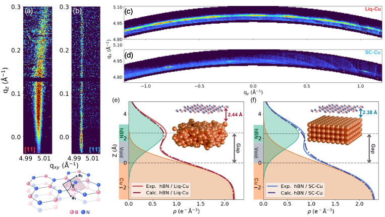
GID probes the 2D Bragg rods that are the fingerprint of a single atomic sheet, giving access to the crystallinity of the film, the orientation of its domains in the plane, and their size (Figure 1a-d). XRR complements this by probing the layer out of plane, returning an electron-density profile that establishes the number of layers and the spacing between hBN and the copper beneath it (Figure 1e-f). These measured geometries were compared to atomistic simulations facilitated by machine-learned interatomic potentials, themselves trained on first-principles calculations, linking the van der Waals gap directly to the microscopic interaction between film and substrate.
Click figure to enlarge
Fig. 1: Reciprocal-space detector images of the hBN [11] 2D Bragg rods for layers grown on (a) molten (Liq-Cu) and (b) re-solidified single-crystal copper (SC-Cu); qxy and qz are the in-plane and out-of-plane momentum transfers, respectively. The inset shows the honeycomb hBN lattice (boron in pink, nitrogen in blue). (c,d) The same rods seen from above, with intensity summed along qz to give a qx-qy map in which each spot corresponds to an individual diffracting grain. Liq-Cu (c) produces a near-continuous arc, the signature of a polycrystalline film with grains oriented in all directions, while SC-Cu (d) shows only a few discrete orientations, indicating an epitaxially aligned film with larger crystalline domains. (e,f) Electron-density profiles along the surface normal for hBN on Liq-Cu and SC-Cu, measured experimentally (solid lines) and from atomistic simulations (dash-dotted lines). The sketches illustrate the difference in hBN-Cu spacing: 2.44 Å on Liq-Cu against 2.38 Å on SC-Cu. Adapted from original publication.
Contrary to expectations, Liq-Cu yielded 3D outgrowth, with grains oriented in all directions and averaging only ~0.1 µm across, whereas the SC-Cu surface produced high-quality, epitaxially aligned films that mainly consisted of a single layer, with domains roughly twice as large (~0.2 µm). XRR measurements traced the origin of the difference at the interface itself, where hBN sits 2.44 ± 0.06 Å above Liq-Cu but 2.38 ± 0.05 Å above SC-Cu. Both values were measured at growth temperatures (1370 and 1355 K), and the offset between them is systematic across datasets and reproduced by the simulations. Graphene shows no such distinction.
Calculations point to a directional, boron-specific bonding component at the hBN-Cu interface, something an ordered crystal surface stabilises particularly well. The deciding factor is therefore not the phase of the substrate itself but the adhesion strength of the layer, which translates to the adsorption height as a measurable descriptor. Interfacial stabilisation thus joins macroscopic considerations such as precursor solubility in copper among the factors that decide whether growth remains monolayer, as targeted for nanoelectronics applications, or proceeds to multilayer growth.
The impact
Resolving crystalline and interfacial structure while a 2D film is still growing gives quantitative access to a buried interface that has remained largely out of reach on a liquid catalyst. Knowing how strongly a layer binds to its substrate explains why a catalyst that is ideal for one 2D material can favour multilayer/3D growth rather than monolayer formation in another. Rather than narrowing the case for liquid metal catalysts, this identifies the parameter that decides which catalyst phase suits which material. Interfacial adhesion, alongside macroscopic factors such as precursor solubility, thus becomes a tunable design parameter in catalyst selection, opening a route to the scalable synthesis of uniform dielectric films for van der Waals nanoelectronics.
Principal publication
Hexagonal Boron Nitride on Liquid and Single-Crystal Copper: Operando X-Ray and Atomistic Insights into Growth and Interfacial Structure, N. Ghanadan et al., Adv. Sci. e76354 (2026); https://doi.org/10.1002/advs.76354
References
[1] M. Jankowski et al., ACS Nano 15, 9638-9648 (2021).
[2] M. Saedi et al., Rev. Sci. Instrum. 91, 013907 (2020).
|
About the beamline: ID10-SURF The beamline operates from 7 to 30 keV with Si(111) optics and from 14 to 30 keV with Si(311), reaching an unfocused beam of less than 1 × 0.5 mm2 and less than 0.03 × 0.1 mm2 when focused. Length scales from below a nanometre to roughly 100 nm are accessible, which makes the station suited to buried and liquid interfaces that cannot be reached by electron- or scanning-probe methods. Combined with a dedicated high-temperature CVD reactor, these capabilities allow the structure of a 2D film and of its interface with a molten catalyst to be followed while growth is under way. |
Top image: Illustration by Marie Najean
partners


European Synchrotron Radiation Facility - 71, avenue des Martyrs, CS 40220, 38043 Grenoble Cedex 9, France.