- Home
- News
- Spotlight on Science
- Organic photovoltaic...
Organic photovoltaic device local structure revealed by combined X-ray diffraction and fluorescence
25-09-2013
The detailed structure of post-fabricated multilayered organic electronic devices has been revealed by an in situ spatially-resolved study, using vertical scanning X-ray diffraction combined with fluorescence spectroscopy. The mechanisms leading to the structural properties of the different organic layers and interfaces could be interpreted. This experimental investigation prepares the way for in situ diagnosis of nanolayered structures.
Polymer-based materials are ubiquitous in almost every aspect of modern society. Their interest arises from their simple chemical processing and the low-cost fabrication of thin films via vacuum evaporation or solution casting technologies. Polymer-based organic photovoltaic devices have potential for the creation of inexpensive renewable energy sources with low environmental impact. Their advent would mean the introduction of a cheap and efficient means to produce electricity from sunlight.
Tremendous progress in organic photovoltaic devices has been achieved with the introduction of bulk heterojunction solar cells based on donor-acceptor blends, typically a conjugated polymer and a soluble fullerene derivative [1-3]. However, device efficiency has not yet reached the maturity level needed to cope with the stringent requirements of routine industrial production. The two fundamental limiting factors are the comparatively low optical absorption of ultrathin photoactive layers, and the practical impossibility of enhancing the absorption by increasing the thickness of the active layer due to bulk recombination losses. The latter is mainly caused by the poor charge carrier diffusion in the organic materials and the sandwich-type geometry of organic photovoltaic cells. Novel solutions must therefore be found to harvest light in a more efficient way. A promising approach is the use of plasmonic metallic nanoparticles, which strongly absorb light in the UV–visible band. This feature is attributed to the localised surface plasmon resonance between the nanoparticles surface electrons and the light electromagnetic field. In this respect, plasmonic nanoparticle-based organic photovoltaic devices could herald a technological revolution toward high performance and durable solar cells [2,3].
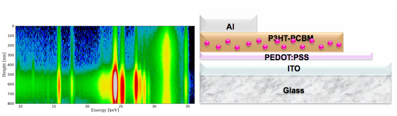
An unprecedented experiment combining X-ray diffraction (XRD) and fluorescence (XRF) with nanometre resolution on post-fabricated organic photovoltaic devices doped with gold nanoparticles was performed at beamline ID11. By scanning the organic photovoltaic cell cross-section with a ~100 nm focused X-ray beam, the structural properties of the different layers and interfaces comprising the device as well as the nanoparticle distribution were studied in situ.
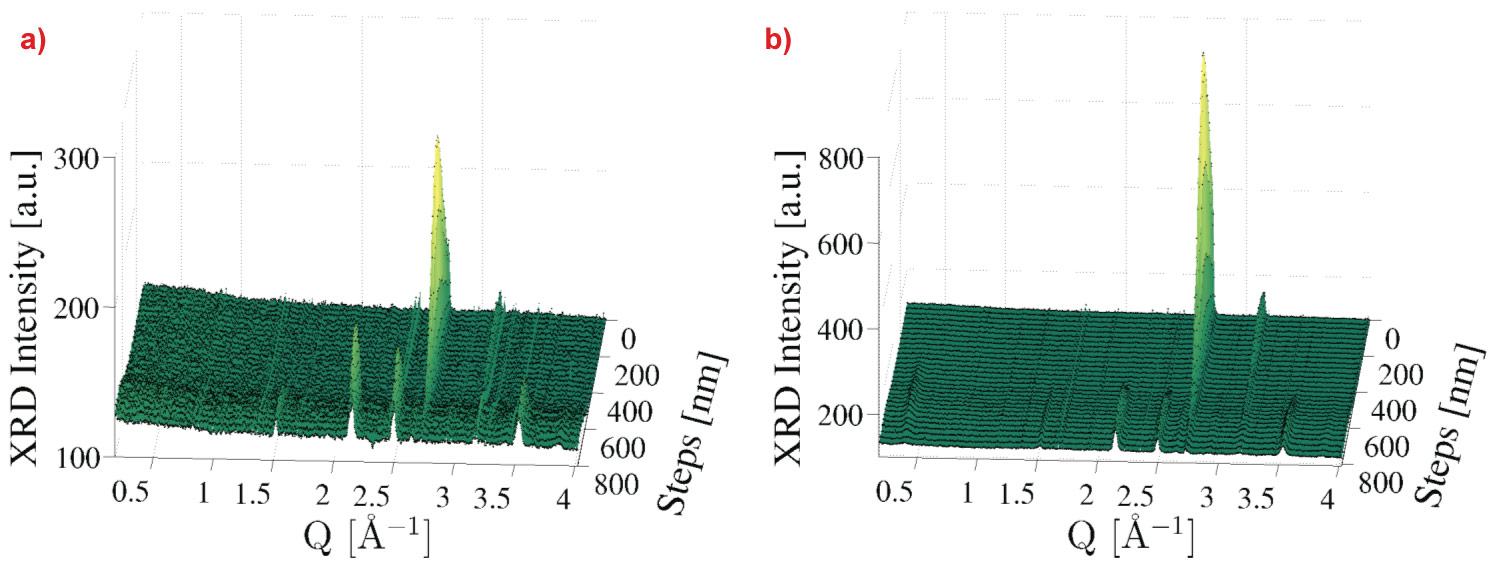
The general scheme for the organic photovoltaic cell used for the experiment is shown in Figure 1. During the measurements, the device was translated vertically through the X-ray beam, from the aluminium top electrode to the indium tin oxide (ITO) layer, while X-ray diffraction patterns were recorded continuously. As the beam size was comparable to the thicknesses of the different layers, the scanning procedure allowed discrimination of the diffraction signals from the individual layers. Waterfall diagrams of the collected diffraction patterns are reported in Figure 2a-b.
 |
|
Figure 1. Schematic diagram of the organic photovoltaic cell used for the experiment. |
The measurements provided an accurate space-resolved description of the molecular ordering of the polymer component of the photo-active layer. Such information is crucial, since the photovoltaic energy conversion rate strongly depends on the nanoscale phase separation during the donor/acceptor heterojunction formation as well as the nanomorphology of the interfaces formed between the active and the charge-collecting layer.
 |
|
Figure 2. Waterfall diagrams of the XRD patterns collected for the as-prepared and the annealed state of the test device, respectively. |
The accuracy of the experimental technique made it possible to measure the nanoparticle distribution profile across the device thickness. Discerning the gold nanoparticle distribution inside the active layer and at its buried interface is essential to understand the contribution of localised surface plasmon resonance to the device's efficiency. New insight has been gained into the role of plasmonic nanoparticles and, as such, may be considered as a milestone towards a better understanding of how the performance of organic photovoltaic cells is correlated to the morphology of their respective components on the nanoscale, an essential step towards new strategies for the development of highly efficient devices.
Thermal annealing performed in situ during the X-ray experiment allowed the monitoring of changes in the nanoparticle distribution and structural properties of the organic layer as a function of the device depth. The results uncovered the chemical-physical phenomena such as modification of the local nanostructure and organisation, interface effects and interdiffusion processes, which occur as a consequence of the annealing process that is used to optimise organic solar cell efficiency. These results are in agreement with the photovoltaic characteristics (calculated from the measured current–voltage characteristics under AM1.5 solar simulator), i.e. the significant improvement of the photovoltaic performance for the annealed devices when compared to that of pristine devices, whereby annealing almost quadruples the photovoltaic efficiency.
The simultaneously performed XRF measurements are consistent with XRD findings and corroborate them. The fluorescence line intensities are shown in Figure 3 versus the vertical scanning step for each metallic element in the device. One interesting effect of the thermal annealing is interdiffusion from the ITO into the polymeric hole transporting layer (PEDOT:PSS), in agreement with the existing literature. From the observations one can infer that, in the present case, indium diffusion may take place within ~15 nm from the ITO/PEDOT:PSS interface.
 |
|
Figure 3. Fluorescence line intensities versus the vertical scanning tracking each metallic element in the organic photovoltaic device. |
These results represent a big step towards the elucidation of structure-property relations that link different length scales, from local nano/hetero structures and interfaces to large-scale devices. The high spatial resolution achieved at the ID11 beamline of the ESRF made these studies possible. With forthcoming advances in modern nanofocusing X-ray optics, it should be possible to study virtually any type of multilayered organic electronic device on all relevant length scales.
Principal publication and authors
Spatially resolved in situ structural study of organic electronic devices with nanoscale resolution: the plasmonic photovoltaics case study, B. Paci (a), D. Bailo (a), V. Rossi Albertini (a), J. Wright (b), C. Ferrero (b), G.D. Spyropoulos (c,d), E. Stratakis (d), E. Kymakis (c), Advanced Materials 25, 4760–476 (2013).
(a) Istituto di Struttura della Materia, C.N.R., Rome (Italy)
(b) ESRF
(c) Technological Educational Institute of Crete, Heraklion (Greece)
(d) Foundation for Research and Technology-Hellas and University of Crete, Heraklion (Greece)
References
[1] A.C. Mayer, S.R. Scully, B.E. Hardin, M.W. Rowell, M.D. Mc Gehee, Mater. Today 10, 28 (2007).
[2] B. Paci, A. Generosi, V. R. Albertini, G. D. Spyropoulos, E. Stratakis, E. Kymakis, Nanoscale 4, 7452 (2012).
[3] B. Paci, G.D. Spyropoulos, A. Generosi, D. Bailo, V.R. Albertini,, E. Stratakis and E. Kymakis, Adv. Funct. Mater., 21, 3573 (2011).
Top image: In situ spatially-resolved X-ray study of an integrated organic photovoltaic device at beamline ID11
partners


European Synchrotron Radiation Facility - 71, avenue des Martyrs, CS 40220, 38043 Grenoble Cedex 9, France.