- Home
- News
- Spotlight on Science
- The resistive switching...
The resistive switching mechanism of CBRAM clarified by XAS
24-11-2015
Ag:GeSx-based conductive-bridging random-access memory (CBRAM) were characterised using synchrotron techniques before and after electrical switching. These experiments gave fundamental insight into the diffusion phenomenon of Ag+ in Ag-GeSx glass and the structure of the solid electrolyte used in CBRAM devices.
In recent years, resistive random-access memories (RRAM) have received extensive interest since they constitute promising candidates for future data storage and information technologies with applications such as non-volatile memories and neuromorphic computing. Among the different approaches, CBRAM based on an Ag:GeSx glass sandwiched between an Ag electrochemically active anode and an inert cathode are considered as one of the most promising technologies [1]. Under the influence of an electric field, it is supposed that Ag ions are produced at the anode and migrate in the electrolyte to form a conducting path. This process is reversible by applying an opposite bias. However to date, the lack of understanding of the switching mechanisms at a nanoscale level prevented the successful transfer of such a technology to industry. In this context, we report the characterisation of Ag/GeSx/W CBRAM devices using synchrotron techniques.
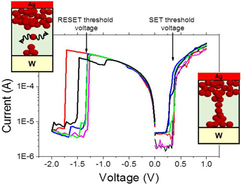
Our approach was based on the design of CBRAM devices specifically-adapted in order to be finely characterised depending on their resistive states by means of depth-selective X-ray absorption spectroscopy (XAS) at the LISA-CRG beamline, BM08. The CBRAM devices were tested electrically prior to the experiment in order to simulate a memory in its different states (electrically switched or not). The devices consist of a GeSx electrolyte layer (50 nm) deposited on a tungsten bottom electrode (25 nm) and covered by an Ag active top electrode (20 nm). After switching, the Ag top electrode was completely removed by ion beam etching prior to the XAS experiments. Figure 1 illustrates the typical I(V) curves obtained and the reversible switching from the high to the low resistive state (SET and RESET, respectively).
 |
|
Figure 1. Typical I(V) curves of a CBRAM device during cycles of SET and RESET between the low and high resistive states. Four cycles are reported in this example. |
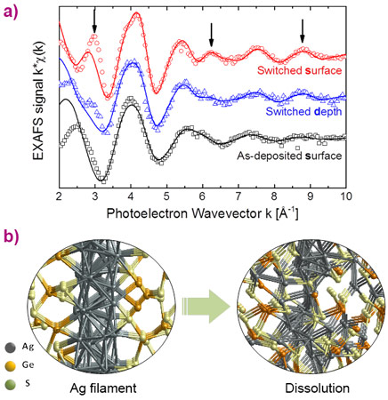
Figure 2a shows the XAS spectra depending on the switching state of the device and on the depth within the sample from which the signal originated. CBRAM that never underwent any switching shows a lower silver metal fraction whereas the switched ones present a higher value. Moreover, XAS surface data show a higher metal fraction below the anode in comparison to the entire layer. Our experiments highlight that the switching process involves the formation of metallic Ag and the formation of this phase is initiated at the Ag electrode. This supports a model of the formation of nanofilaments consisting of Ag metallic cones with their base on the active electrode as metal reduction happens more rapidly than ion migration. Moreover, the study of the local environment around Ag atoms in such devices reveals that Ag is in two very distinct environments with short Ag-S bonds due to Ag dissolved in the GeSx matrix and longer Ag-Ag bonds related to an Ag metallic phase.
These experimental results are well supported by ab initio molecular dynamics simulations showing that Ag favourably bonds to S atoms. From these results we were able to deduce the origin of the main limitation of this type of devices [2]: the instability of the ON state can be attributed to the sulfidation of Ag and hence rupture of the Ag–Ag metallic conduction path in the GeSx layer.
This work illustrates the importance of using samples specifically designed for characterisation with synchrotron radiation in order to understand the mechanisms involved in the operation of nano-electronic devices. The principle of the nondestructive method described here can be extended to other types of resistive memory concepts (including memristors based on transition metal oxides), and will give fundamental clues about the resistive switching mechanisms.
Principal publication and authors
The role of the local chemical environment of Ag on the resistive switching mechanism of conductive bridging random access memories, E. Souchier (a,b), F. D’Acapito (c), P. Noé (a,b), P. Blaise (a,b), M. Bernard (a,b) and V. Jousseaume (a,b), Phys. Chem. Chem. Phys. 17, 23931 (2015); DOI: 10.1039/C5CP03601A.
(a) Univ. Grenoble Alpes (France)
(b) CEA, LETI, MINATEC Campus, Grenoble (France)
(c) CNR-IOM-OGG c/o ESRF, Grenoble (France)
References
[1] I. Valov, R. Waser, J.R. Jameson and M.N. Kozicki, Nanotechnology, 22 254003 (2011).
[2] E. Vianello et al., Proceedings of the IEEE International Electron Devices Meeting (IEDM) San Francisco, p741 (2012).
Top image: The CBRAM device during an electrical test


