- Home
- News
- Spotlight on Science
- What is between...
What is between the amorphous native oxide layer and the underlying crystalline silicon?
30-04-2015
Silicon surfaces are passivated by a silicon oxide layer. X-ray reflectivity measurements at the ESRF show that the junction between the silicon oxide and crystalline silicon layers has a low density region, for which the reflectivity measurements concord with only the most recent model. Accounting for this low density region will increase the accuracy of future studies of silicon-supported nanoscale layers.
X-ray reflectivity measurements of interfaces involving silicon (001) substrates, widely used in nano applications, reveal a thin low-density layer between the underlying single-crystalline silicon and the native SiO2 layer, a few nm thick, that passivates the surface. Accounting for this layer in structural studies of silicon-wafer-supported mono-layers and few-layer thick films is shown to be crucial for an accurate and high-resolution determination of the surface-normal structure from measurements spanning the extended scattering vector ranges now accessible at the ESRF and other modern third-generation synchrotron sources. Previous measurements, over a more limited range, were not able to establish the existence of a low-density region between the native oxide and the underlying silicon lattice. We speculated that partial hydrogen passivation supports the existence of the low-density region.
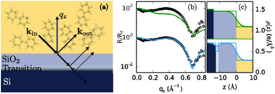
Exploiting high intensity beamlines such as ID10 and ID15A at the ESRF, our study elucidated, for the first time and with sub-angstrom resolution, the structural aspects of the junction between the truncated crystal lattice of silicon and its amorphous native oxide layer. The interface between such a substrate and a simple organic liquid (bicyclohexane) is shown in the cartoon in Figure 1a, highlighting also the multiple reflections of incident X-rays from the various interfaces. Interference of the reflected rays in the far field generates a modulated reflectivity curve which is then used to extract the surface-normal electron-density profile. Such a reflectivity curve is shown in Figure 1b.
The importance of accounting for the transition layer in modeling the silicon/liquid interface is demonstrated by comparing fits of the measured reflectivity curve in Figure 1b from models including this layer (blue) and a widely used older model [1], which excluded this layer. The experimentally-refined lower density of this layer, corresponding to 6-8 missing electrons per silicon unit cell area, supports previous theoretical models and simulations of the Si/SiO2 interface [2].
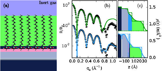
Figure 2 shows reflectivity measurements for the much more complex interface of the same wafer, covered by an OTS (octadecyltrichlorosilane) monolayer, self-assembled by the standard method of immersion in an OTS/BCH solution, then extracted, washed, and dried. Figure 2a highlights the larger number of X-ray-reflecting interfaces in this sample as compared to Figure 1a. Yet, a model accounting in detail for our recently-discovered headgroup structure [3], and for the low-density layer at the Si/SiO2 interface perfectly reproduces (blue line) the measured reflectivity (symbols) over the full range of scattering vectors measured. By contrast, the older model [1] which excludes the low density layer and the headgroup structure (green line), provides a much poorer fit, reproducing reasonably only the lower half of the now-measurable range of scattering vectors.
The inclusion of a depletion layer at the Si/SiO2 interface in the model discussed above is also motivated by the different oxidation states found for silicon at the Si/SiO2 interface resulting from the mismatch in bond density between Si and SiO2 [4]. Furthermore, theoretical studies also predict an interfacial layer with reduced density, attributed inter alia to voids at the Si/SiO2 interface in the Si-O-Si bridge bonds model [2].
Our results provide for a significant increase in the resolution and accuracy with which the surface normal structure of silicon-supported nanoscale layers can now be determined by X-ray reflectivity. As these layers play an important role in both the basic science and the technology of a broad range of nanoscale devices and constructs, this study should benefit many disciplines. We also hope that this study will stimulate further theoretical, simulation and experimental research of other related systems.
Principal publication and authors
Nanoscale structure of Si/SiO2/organics interfaces, H.-G. Steinrück (a), A. Schiener (a), T. Schindler (a), J. Will (a), A. Magerl (a), O. Konovalov (b), G. Li Destri (b), O.H. Seeck (c), M. Mezger (d), J. Haddad (e), M. Deutsch (e), A. Checco (f), and B.M. Ocko (f), ACS Nano 8, 12676 (2014).
(a) Crystallography and Structural Physics, University of Erlangen-Nürnberg, Erlangen (Germany)
(b) ESRF
(c) HASYLAB am DESY, Hamburg (Germany)
(d) Max Planck Institute for Polymer Research, Mainz (Germany)
(e) Physics Department, and Institute of Nanotechnology and Advanced Materials, Bar-Ilan University, Ramat-Gan (Israel)
(f) Condensed Matter Physics & Materials Science Department, Brookhaven National Laboratory, Upton NY (United States)
References
[1] I.M. Tidswell et al., Phys. Rev. B 41, 1111 (1990).
[2] Y. Tu and J. Tersoff, Phys. Rev. Lett. 84, 4393 (2000).
[3] H.-G. Steinrück, A. Magerl, M. Deutsch and B.M. Ocko, Phys. Rev. Lett. 113, 156101 (2014).
[4] T. Hattori, Crit. Rev. Solid State Mater. Sci. 20, 339 (1995).
Top image: Illustration of the interface between a silicon wafer and a self-assembled octadecyltrichlorosilane monolayer.


