- Home
- Users & Science
- Scientific Documentation
- ESRF Highlights
- ESRF Highlights 2001
- Methods and Instrumentation
- Microcrystallography with an X-ray Waveguide
Microcrystallography with an X-ray Waveguide
X-ray microdiffraction experiments on the micrometre scale are now routinely performed at third-generation synchrotron radiation sources, such as ESRF [1]. With this in situ technique, samples can be scanned with microscopic positional resolution. There is growing interest in achieving even smaller beam sizes in the sub-micrometre range in order to investigate structural details on mesoscopic length scales, i.e., between microscopic (micrometres) and atomic distances (nanometres). Examples include biomaterials, polymers and phase analysis in inhomogeneous mixtures (see below).
X-ray waveguide optics is a promising approach for sub-micrometre crystallography. These devices have been shown to provide beams of 0.1 µm in one dimension [2]. The waveguide used in the present study has a Mo/C/Mo sandwich structure with a carbon spacer of 80 nm. Radiation transport in the waveguide takes place through the light element layer by total reflection at the opposing metallic layers. The experiment was carried out on ID13, the Microfocus Beamline, at an energy of 13 keV. A graded multilayer mirror was used to focus the beam horizontally to 3 µm while the waveguide focussed the beam to 0.1 µm in the vertical direction. The flux at the sample position is 109 photons/s in the 0.1 x 3 µm2 spot at a storage ring current of 200 mA. The scanning setup developed at ID13 is shown in Figure 161. Two video microscopes allow for precise sample alignment. A three-axis piezo translation stage enables positioning and scanning of the sample with better than 0.1 µm repeatability.
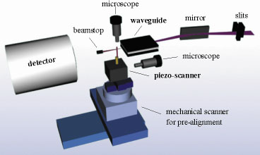 |
Fig. 161: Schematic view of the sub-micrometre scanning setup on ID13 with combined mirror and waveguide optics. |
When compared with standard experiments using large beam sizes, X-ray microdiffraction on phase mixtures can give more interesting and informative results. A rough classification of the expected scattering patterns is possible by comparing the beam size (S) with the size of the coherently scattering object (L):
1. L > S means single crystal diffraction with only a few spots on the detector.
2. For L ~ S one expects the presence of spikes on the Debye-Scherrer (powder) rings.
3. L < S implies powder rings.
As an example for all of these cases, we chose a grain from the handle of a Koan transport amphora used during the period 300 BC to 100 AD. It shows a complex phase mixture, which is typical for ceramics samples. The scanning electron microscope (SEM) image (Figure 162a) suggests compositional changes on different length scales. Correspondingly, the diffraction pattern (transformed to polar coordinates, Figure 162b) shows that the size of coherently scattering objects varies considerably. Spikes are an indication for scattering objects of the same size as the beam (case 2); weaker continuous lines below the spikes suggest the presence of fine powder grains (case 3); in addition, strong reflections from larger single crystallites are observed (case 1).
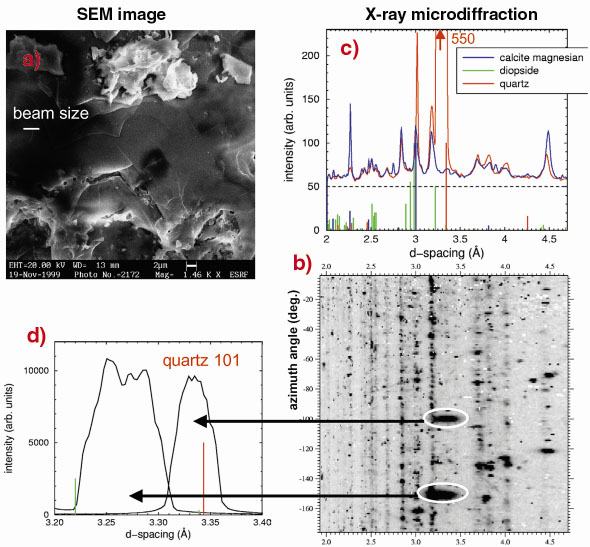 |
Fig. 162: SEM and X-ray microcrystallography results for a grain from the handle of a Koan transport amphora. |
The two averaged powder patterns shown in Figure 162c were collected at sample positions that are 17 µm apart. The calculated positions of reflections suggest the presence of magnesian calcite, diopside and quartz. The strong 101 quartz reflection (red curve of Figure 162c) is clearly visible as a prominent single crystal reflection (Figures 162b and 162d). The present data demonstrates that with sub-micrometre beam sizes the signals from small amounts of a rare component can be detected and discriminated against the strong contributions of quartz or calcite.
References
[1] C. Riekel, Rep. Prog. Phys., 63, 233-262 (2000).
[2] A. Cedola, S. Lagomarsino, S. Di Fonzo, W. Jark, C. Riekel and P. Deschamps, J. Synchrotron Rad., 5, 17-22 (1998).
Principal Publication and Authors
M. Müller (a,b), M. Burghammer (a), D. Flot (a), C. Riekel (a), C. Morawe (a), B. Murphy (c,b) and A. Cedola (d), J. Appl. Cryst., 33, 1231-1240 (2000).
(a) ESRF
(b) now at: Institut für Experimentelle und Angewandte Physik, Universität Kiel (Germany)
(c) Daresbury Laboratory, Warrington (UK)
(d) Instituto di Elettronica dello Stato Solido, Roma (Italy)
partners


European Synchrotron Radiation Facility - 71, avenue des Martyrs, CS 40220, 38043 Grenoble Cedex 9, France.