- Home
- Liquid phase epitaxy facility for single crystal film scintillators
Liquid phase epitaxy facility for single crystal film scintillators
2D X-ray detectors for synchrotron sources have become a standard for almost all applications including radiography and tomography. High-resolution detectors are able to provide volumetric data of samples during non-destructive experiments for biology, medicine and material sciences. They can also be used as diagnostic tools for the X-ray beam. A detector that is able to provide sub-micrometre spatial resolution consists of a scintillator, light microscopy optics and an image sensing device (CCD or CMOS). The scintillator converts the X-rays into visible light which is projected onto the image sensor through the optics. Sub-micrometre resolution requires a thin layer, in the micrometre thickness range, with a high optical grade for the sensitive layer. The thinner the scintillator film, the better the spatial resolution and image contrast. Thin film layer growth requires the use of several advanced techniques: sputtering, chemical solution deposition, liquid phase epitaxy (LPE), laser ablation, etc. As such single crystal film (SCF) scintillators are not commercially available, the ESRF has constructed its own scintillator production facility with LPE capability. LPE is a versatile technique for the development of miniature optical components, such as lasers, amplifiers and scintillators, in single crystal structures [1]. This technique was chosen owing to its high reproducibility, simplicity and homogeneous distribution of the activator ions within the film.
The 40 m2 laboratory has been operational since April 2010 and is divided into three main sectors: Chemistry room for powder and substrate preparation, a “lead oxide” room for the manipulation of micro-nano toxic powders and a furnace room.
We have already produced some europium-doped gadolinium gallium garnet (Gd3Ga5O12:Eu; GGG) films for the ESRF beamlines. The constituents of the solution are melted in a platinum crucible at about 1000°C. Before growth, the melt is stirred at about 1100°C. The substrate is mounted horizontally on a platinum holder and preheated in the furnace.
 |
|
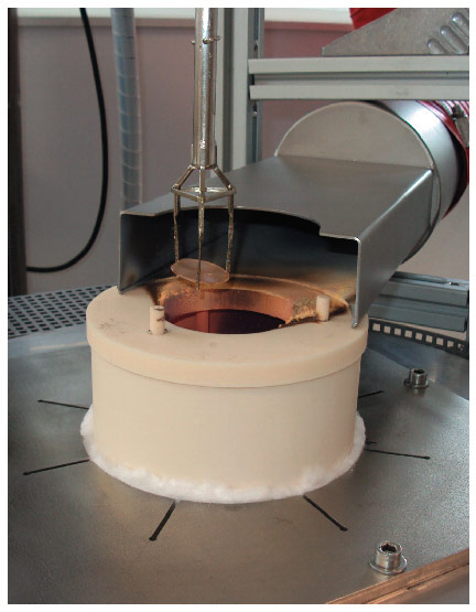
Fig. 145: SCF scintillator, after growth and melt characterisation, fixed on its platinum holder. |
The growth is then performed at constant temperature by dipping the substrate in the supersaturated melt solution (Figure 145). The single-crystal films from 2 µm to 120 µm that have been manufactured show high optical quality (Figure 146) and have the same level of performance as layers developed previously in the now-defunct laboratory of a partner institute.
 |
|
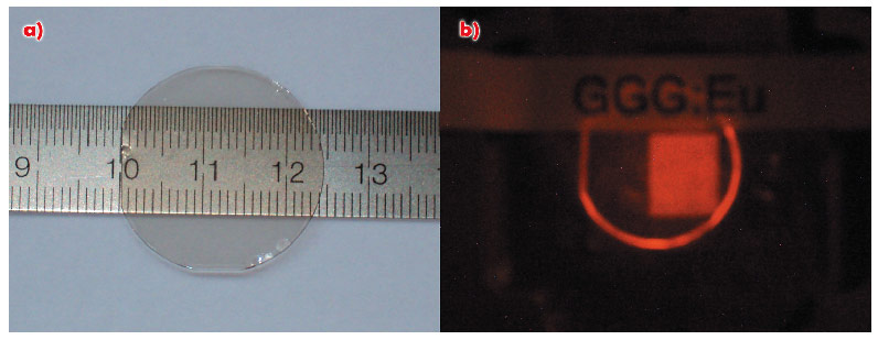
Fig. 146: An ESRF GGG:Eu scintillator. a) 16 µm thick GGG:Eu on 500 µm undoped GGG, 25.4 mm diameter. b) Digital camera picture of visible light emitted by the scintillator under irradiation from a laboratory X-ray generator (40 kV, 40 mA). |
Today the thin scintillators that are the most promising to reach spatial resolution in the micrometre range suffer from inadequate detection efficiency. There is therefore a need to develop more efficient SCF scintillators made from materials of high density and high effective atomic number. In a first step, we have chosen candidate materials that are garnet and silicate based. At a later stage, we may try materials based on peroskite, hafnate, tantalate and lutetium. In particular, gadolinium and lutetium oxide are more promising host materials than GGG because of their high density. Lutetium oxide could boost the absorption efficiency by a factor of 2 or 3 when compared to GGG and YAG, respectively. These materials could provide even higher absorption efficiency than the garnet and silicate based materials, but today they are much less well known because of the lack of substrates and/or temperature of growth. We successfully developed a scintillator based on GGG:Tb at the end of 2010, which provided a better wavelength emission that matches interline and back-illuminated CCD chips. Optical quality and light yield are promising for the future production of GGG:Tb in 2011. An investigation of dense garnet materials was also launched in 2010: pure LuGG substrates are under development and the first LuGG:Eu layer is expected in the first half of 2011. For LuGG co-doped with a weak concentration of terbium, the sensitivity of detectors coupled to back-illuminated CCD will be improved by a factor of 4 in comparison with GGG:Eu. While we are able to perform significant development work in-house, international collaborations would be welcomed concerning substrates and the growth of exotic materials.
To conclude, the LPE facility is operational for production and development. The SCF scintillators that we have produced provide sub-micrometre resolution with high contrast. The alternative materials tested so far, such as YAG, LuAG, GGG and LSO, show complementary performance. This new facility aims to be of great benefit to the synchrotron community and will ensure continuous production, innovation and development for X-ray imaging and other applications. Our scintillators are available for the ESRF beamlines and are also commercially available [3].
Authors
T. Martin, P.-A. Douissard and E. Mathieu.
ESRF
References
[1] B. Ferrand, B. Chambaz and M. Couchaud, Optical Materials 11, 101-114 (1999).
[2] P.A. Douissard, A. Cecilia, T. Martin, V. Chevalier, M. Couchaud, T. Baumbach, K. Dupré, M. Kühbacher and A. Rack, J. Synchrotron Rad. 17, 571-583 (2010).
[3] For details please contact: ESRF Industry Solutions
Acknowledgement
The authors thank the CEA/LETI and especially M. Couchaud, A. Million and J.L. Santailler for their help and advices in the LPE laboratory installation. We also thank the ESRF Technical Service and Safety Group for their work and support.
partners


European Synchrotron Radiation Facility - 71, avenue des Martyrs, CS 40220, 38043 Grenoble Cedex 9, France.